In the last post we settled on a controller card to run the laser projector. But to control XY, color, shutter, and etc. we are going to need some DAC and digital control channels. Based on the ILDA projector specification and our measurements, I believe we will need the following MCU channels:
| Channel | Type | Description | Output |
|---|---|---|---|
| 1 | DAC Output | X | -5~5 |
| 2 | DAC Output | Y | -5~5 |
| 3 | DAC Output | R (C1) | 0~5 |
| 4 | DAC Output | G (C2) | 0~5 |
| 5 | DAC Output | B (C3) | 0~5 |
| 6 | DAC Output | C4 | 0~5 |
| 7 | DAC Output | C5 | 0~5 |
| 8 | DAC Output | C6 | 0~5 |
| 9 | Digital Output | Intensity/Blanking | 0/5 |
| 10 | Digital Output | Shutter | 0/5 |
| 11 | Digital Input | DMX RX | 0/5 |
| 12 | Digital Output | DMX TX | 0/5 |
| 13 | Digital Output | Sync Out | 0/5 |
| 14 | Digital Input | Sync Input | 0/5 |
Note, in the ILDA specification a number of these signals are differential. That is, there isn’t just an X signal, but an X+ and X- signal. We’ll address this on our IO board, but that isn’t something that the MCU will be concerned with.
There are also a number of signals that aren’t in the spec and which we haven’t mentioned yet. So let’s review the signal groups one at a time. But first, let’s go over our basic PCB platform.
The PCB and Dev Board Connection
As I mentioned in the last post, our STM32F769 based eval board has a connector for Arduino expansion modules. Arduino is an open source hardware and software company whose microcontroller offerings are generally based on the older Atmel (now Microchip) AVR AtMega processors.
Although I am familiar with the AtMega MCUs, the Arduino DIY world is not something I have any experience in and, frankly, is something I don’t want to invest a lot of my all-too-limited supply of remaining neurons on. Still, if we are going to make an IO board based on a standard, we should at least make a cursory effort to comply. Step one would be the physical footprint and connector locations for our PCB.
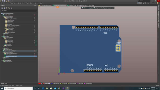
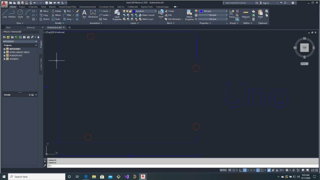
For reasons I don’t understand, Arduino expansion cards are called “Shields“. They are supposed to be the same size and shape as the Arduino board itself for stacking. For reasons I suspect I do understand (cough cough, they want to sell you stuff), the hardware specs are a little hard to access. The official Arduino Uno rev3 link does have a tab for technical documents, but there are less useful than you might expect. For example, the DXF drawing of the PCB does not show connector positions:
There is a schematic in PDF form, but that doesn’t help us. Which leaves “Eagle CAD Files”. Eagle is a proprietary EDA (Schematic/PCB design) tool from Autodesk. I don’t blame anyone for using a proprietary EDA tool. The most popular free tool, KiCAD, is a time wasting sink hole of frustration. The problem I have with Eagle is that it isn’t a tool I own or use. I use Altium Designer, which is pretty much the industry standard these days.
Altium does have an import function that supposedly handles Eagle files, but the Altium manual pages for the function give a bunch of warnings about what will and will not import correctly. So I was little bit nervous when I launched it and input the two files from Arduino but the results were better than I expected:

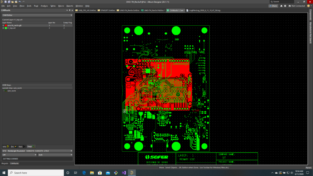
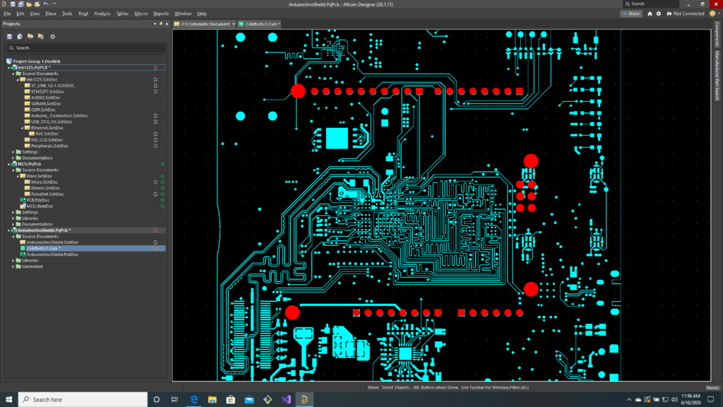
The schematic looked pretty close to the PDF version and, while silkscreens and other text were whack, the basic copper and drill areas of the PCB looked reasonably correct. ST lets you download the PCB gerber files for the dev board we are using, so I lined those up with the imported Arduino board to make sure everything aligned correctly:
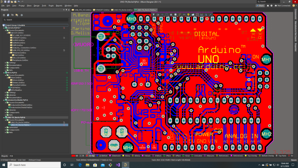
I was just about to go through the somewhat tedious process of putting together a new board based on the dimensions and part placement of the imported Arduino board when I found that someone had already done this and posted the files on the Arduino online forums. I pulled that project and checked it against the pinout and gerbers and, again, everything looked fine:
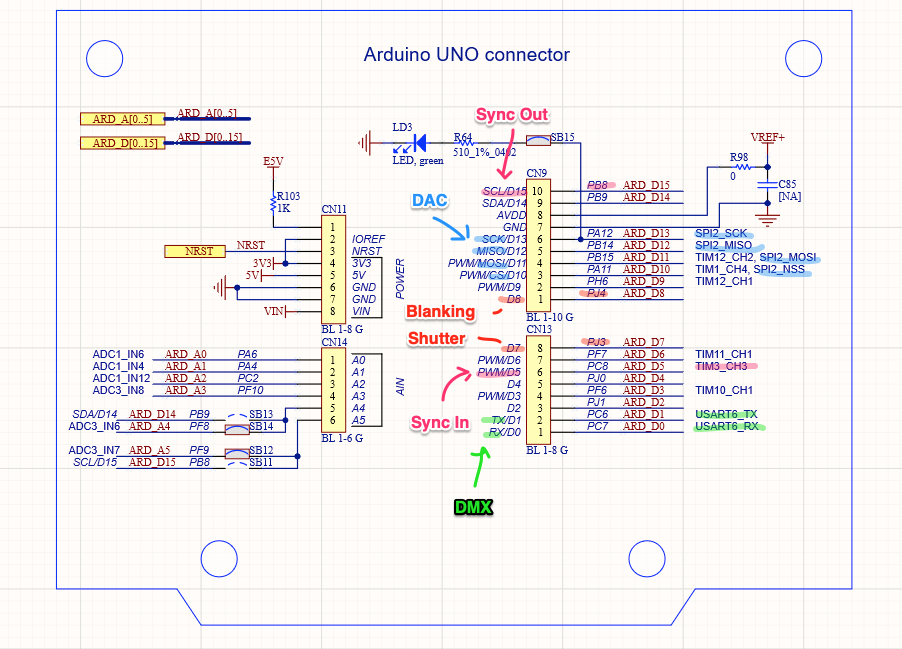
Well done guest user “samarkh”! With our board shape, connector placement, and connector pinout handled, it is time to start looking at our channels. First up, the most critical channels for our ILDA projector.
DAC Channels
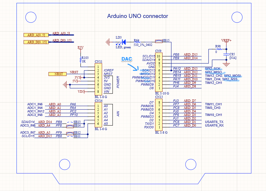
Our first 8 channels are the real core of our laser controller. X/Y position for our scanners and up to 6 channels of color control. The STM32F769 MCU on our control card does have two built in DACs. They are 12 bit (4096 steps) and not horrible, but they are only available on two specific processor pins:
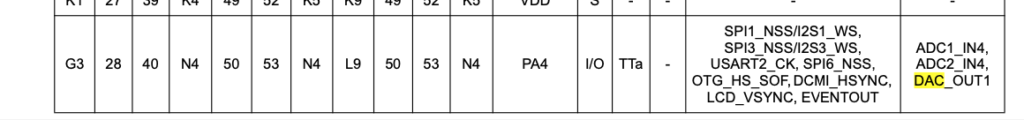
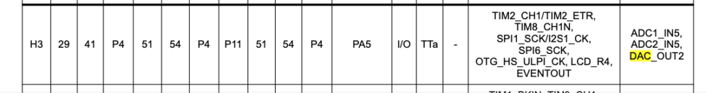
One of those pins does already go to the Arduino expansion connector (PA4 is wired to Arduino A1), but the other, PA5, is used for USB OTG on the board (ULPI CLKOUT):

We are going to want to use that USB connection and 12 bits is a bit lower resolution than I want anyway, so let’s just make our IO board self contained. We can use this 8 channel, 16-bit, SPI controlled DAC from TI.
If we look at the datasheet, we can see that data is output to it serially:
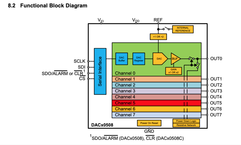
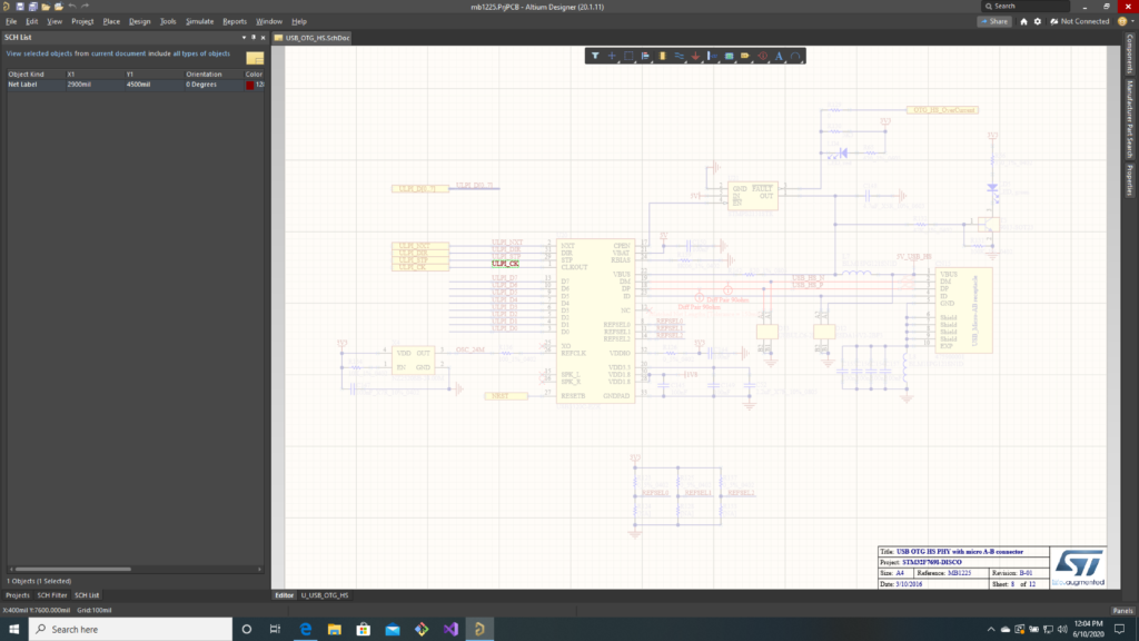
That is, data is clocked to it one bit at a time. If we want to both read and write to the chip the interface is 4 wires (SCLK, SDI, SDO, and CS). If we check the schematic for our eval board we can see that not only are those lines listed on specific Arduino connector pins, they are routed to pins on our processor that can be used for SPI with a built in support peripheral:
If we dig deeper we can see that this setup isn’t perfect. This particular DAC does not offer bulk writing. That is, you can only write to one channel at a time. And the SPI peripheral available, SPI2, is on the slower peripheral bus inside the MCU (see the diagram below), so we will only be able to write to it at 25 MHz, not the 50 MHz it is capable of, but this should still be pretty workable.
This brings up an important point: not all pins on the expansion connector are equal. Some are mapped to pins that can be used with specific peripherals built into the MCU. So I am going to jump out of order a bit and take care of some peripheral specific control channels next.
DMX In and Out
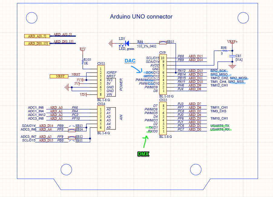
DMX is a standard for controlling theatrical lighting fixtures. It’s clunky and weird with glaring deficiencies (no error checking for packets? wtf!!!) so, of course, it is widely adopted. Basic DMX is unidirectional. Communication only flows in one direction. We will want both a DMX input (DMX RX) so we can be controlled by lighting consoles and a DMX output (DMX TX) so we can control DMX devices. We want this because DMX is often used in laser projectors for beam actuators and motorized effects.
Beneath the DMX protocol is an older serial communication protocol called RS-485. To receive and transmit this protocol you really, really, really want to use a UART (universal asynchronous receiver transmitter) peripheral inside your processor. This is not something you want to do with software and a general purpose IO chip! Trust me, I’ve had to. Thankfully there is a pair of UART pins on the Arduino expansion connectors, so we know where our DMX signals have to be routed! We’ll put RS-485 transceiver chips on our board:
Sync In and Out
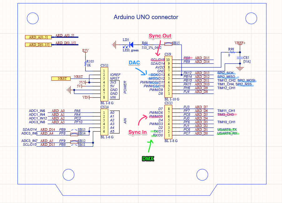
We haven’t really mentioned sync signals before, but we are going to want them. For a typical entertainment application a host computer might be monitoring, say, SMPTE Timecode, and sending trigger signals out to equipment over something like DMX, which is often sending packets at about 40 Hz. This is generally responsive enough for things to look synchronized for an audience, but our first gag is going to be to synchronizing our laser projector with a video camera. In that case we want any link to be much more precisely bound.
Obviously, tying signals directly to the processor doing the scanning will make things more tightly synced than two processors talking over a serial link that is only refreshing 40 times a second. But we want things really tight.
Peripherals typically signal an MCU by generating something called an ‘interrupt’ – stop what you are doing and pay attention to me now. IO pins on most MCU’s can be set to do this as well. We could have our sync in trigger an interrupt. But the response time to an interrupt ‘jitters’. Depending on what the MCU is doing when the interrupt occurs, responding to the interrupt will take varying amounts of time.
That may not be good enough for our purposes, so we are going to connect our sync lines to pins that can be mapped to timer peripherals inside the MCU. You might have noticed that a number the pins are labelled with a specific timer and channel. Channel doesn’t really matter. On our MCU, any timer channel can generally be used as either an input or an output to the timer. But Timer number is another matter. If we look at the datasheet for our MCU I linked to in the last post, we will find this very useful diagram:

If we read the documentation further we will find that the timers are:
- One of different types (“advanced, general purpose, and basic”)
- Reside on either a 54 MHz or 108 MHz peripheral bus
- Only can be synchronized in certain combinations
That last bullet point is key. Based on the notes on ST’s schematic, we basically have 4 timers readily available to us, TIM3, TIM10, TIM11, and TIM12. Timers 10 and 11 look tempting, because they are on the faster peripheral bus (and can actually clock at twice that bus speed), but those timers have almost no synchronization options for use with other timers. Not what we want.
TIM3 is the most flexible in terms of triggering and being triggered by other timers, so we will make it our Sync In. TIM12 can at least be triggered by several of the other timers, so that seems like our only choice for Sync Out, but it is kind of sucky so… we’ll double check the docs instead of just trusting someone’s notes on a schematic!
According the the STM32F7xx datasheet, pins PB8 and PB9 also can be mapped to TIM4, a timer with good synchronization options:

Cool! We will use PB8/TIM4 for our Sync Out:
Shutter and Blanking
Finally, some good old fashioned simple I/O. Our shutter is open or closed and the blanking signal is visible or not. We will just map these to some general purpose I/O pins, though we will want to put a driver chip on our board so our MCU pins aren’t hooked to a long cable:
Now that we have a rough design sketched out, our next step will be to make a proper schematic and PCB!
Leave a Reply