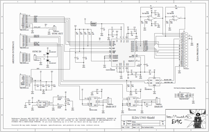
Well, we finally have a schematic for our Arduino UNO compatible ILDA “shield” (PDF version here). It’s pretty close to what we sketched out here. And prototyped here.
A big chunk of the DAC section is just a simplified version of the schematic of the DAC81408 EVM evaluation module we used for prototyping (page 13 here). But there are a few extra sections worth covering briefly.
Power
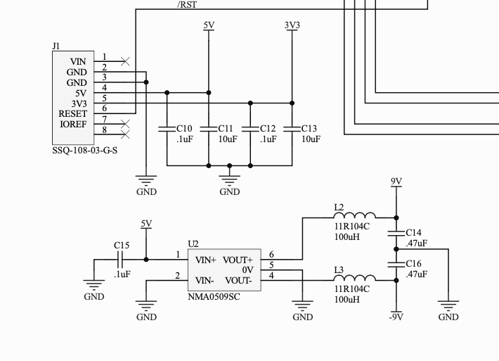
Only 5V and 3.3V come to our board from the host card. In the lower left corner you can see we have some filter caps to clean up the voltages provided and a DC-DC switching converter to provide +/- 9V from 5V in.
We probably could have gotten by with just a 5V to -5V converter, but I was a little concerned that the input impedances of ILDA projectors isn’t really called out in the specification. So I wanted a little extra headroom in case I need to switch op amps to get more drive (more on that below).
Inverting Amplifiers
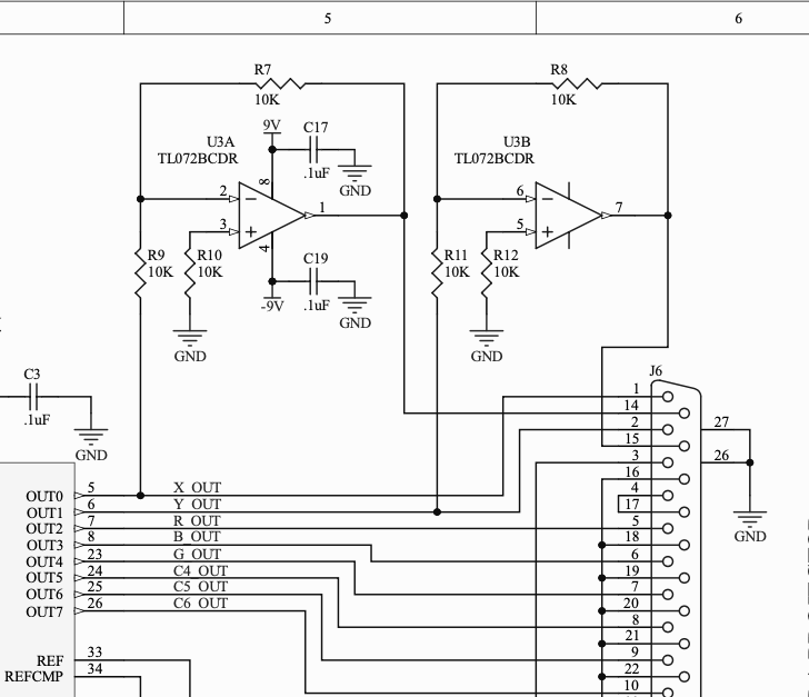
In the top right corner you can see some inverting amplifiers with a gain of 1:1. I used a TL072BCD. It is a common JFET op amp with good harmonic distortion and a fast slew rate. My one concern is that it only has a few milliamps of drive capability. But if this turns out to be a problem the footprint/pinout is common to a number of other amplifiers we can switch in.
If you haven’t worked with op amps, you can download a SPICE model for this one here. LTSpice is a free version of SPICE for Windows that many electrical engineers use. Although it isn’t perfect, simulation is a great way to try things out without prototyping them. In this case, I know that the inverting amplifier will put out an inverted form of the +/-5V signal I put in, but we can still quickly check performance at higher frequencies:
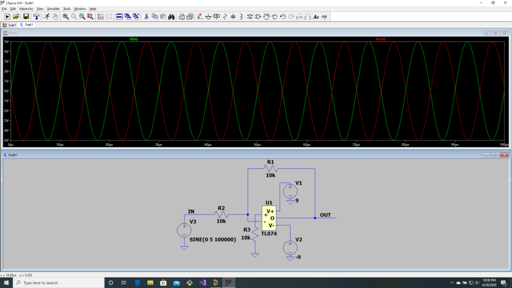
Looks good up to 100 kHz in but, again, my concern is if we have enough output drive capacity for the projector.
Driver Chip
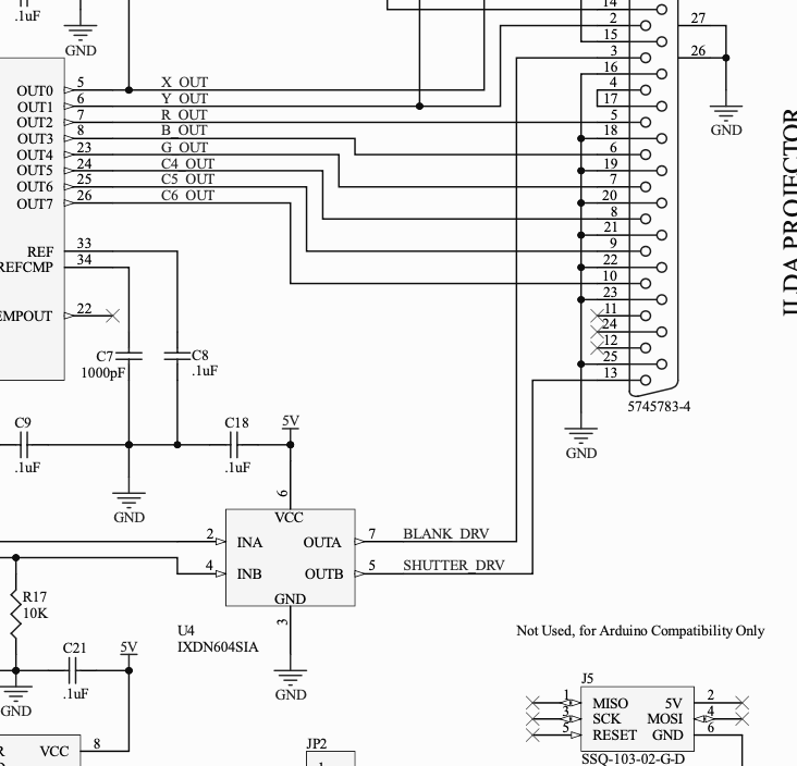
Because a shutter and (possibly) a mechanical intensity control can be inductive loads, there is a two channel driver chip for those signals.
DMX In/Out
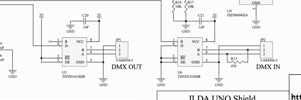
Along the bottom of the schematic is our DMX circuitry. We have a UART controller on the main board, so we only have to provide RS-485 transceivers. These can operate half duplex, but we have one fixed for receiving, the other for transmitting. We also have a termination resistor on our input.
I thought about making our output more sophisticated to support something called Remove Device Management (RDM), but decided to keep the DMX simple for now.
Sync IN and OUT
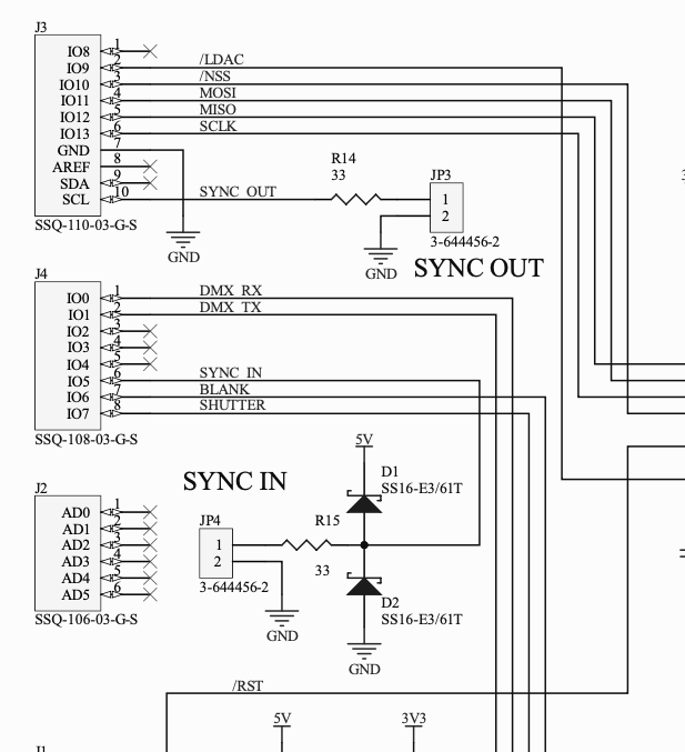
As planned, Sync In and Out are pretty simple general purpose IO from the MCU. Both just have a pad resistor for ringing and a little bit of current protection and the Sync In has some beefy protection diodes added. These do add some capacitance to our input, but it should be fine for the frequencies we are interested in for now, and the extra protection diodes give some piece of mind.
That’s about it. I’ll push everything to the BCM git repo as soon as I wrap up the first revision of the PCB.
Next stop, gerber files…
Leave a Reply