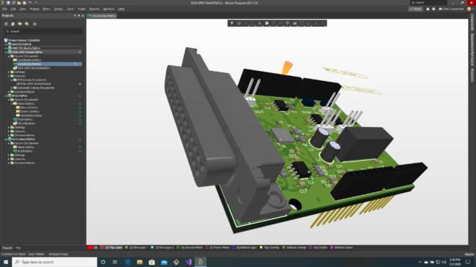
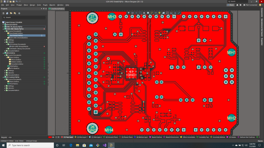
As we say in the last post, our adapter board is pretty simple. So the PCB was quick to route. Most the signal connections on on the top layer:
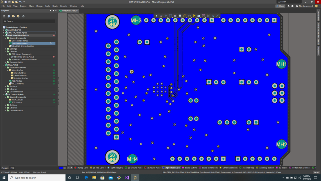
With the SPI signals we use the most (SCLK, MOSI, and NSS) on the back:
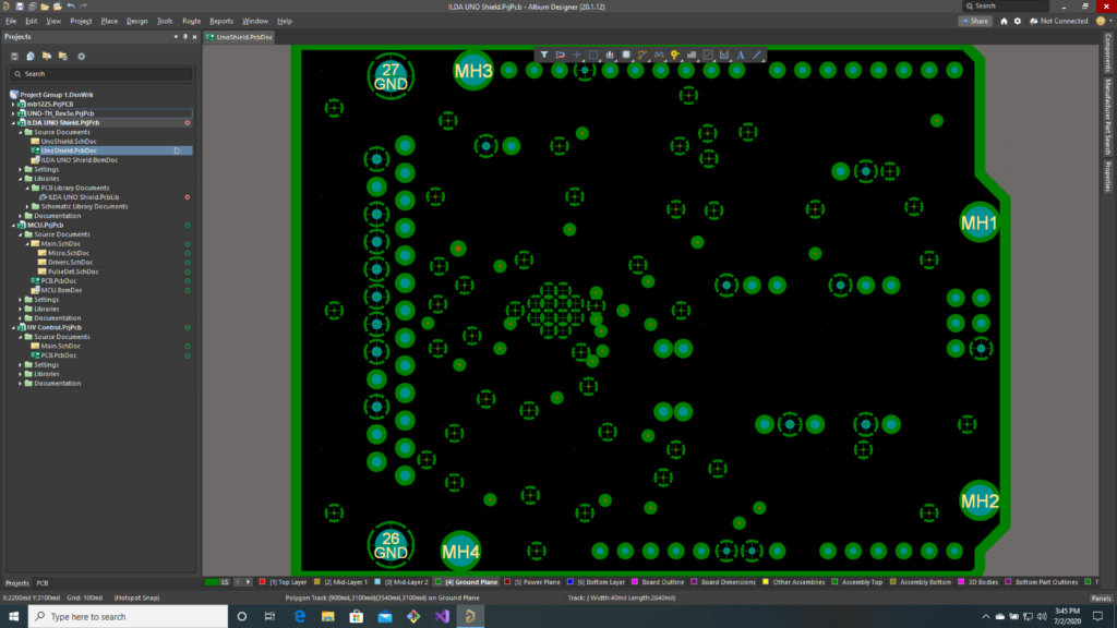
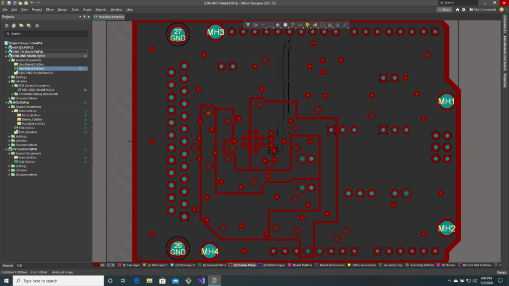
At 25-50 MHz, they are a potential noise source. There is a pretty convention ground plane:
We’ll see what the fabricator’s DFM tool says about all those ground spokes clipped on QFN footprint from TI. Our last layer is a split power plane, with sections for +5V, +9V, -9V, and +3.3V:
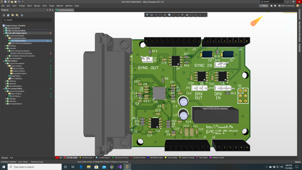
The ILDA projector connection is the big DB-25F at one end. The other connections are on simple .1″ header connectors for now:
Gerbers are generated and submitted for DFM, and everything (Altium design files, library parts, gerber files, etc.) is pushed to the BMC git repo.
Next up, we’ll get a jump start on writing some code while we wait for our prototypes!
Edit: As I feared, the DFM evaluation did not like the footprint for the TI DAC. Internal connections on a PCB generally used “Thermal Reliefs”. The connection is made through little copper spokes so that when the board is being soldered, all the heat does not rapidly transfer to the internal copper planes.
The original footprint had central pad holes that were obliterating most the spokes of other holes nearby, so most of the copper connection was lost. I changed the footprint to an X-pattern:
The board then came back clean:

So I ordered them using the budget special. PCBs should ship back July 13th. I also added a CM (contract manufacturer) quote pack to the git repo. My normal prototype assembler was very reasonable, so I have them setup to do a 1 week turn after boards arrive.
Leave a Reply