This blog isn’t a nice collection of self contained mini articles. It is more of a stream of consciousness while I develop yet another control system for entertainment. Think serialized “Twilight” fan fiction, but shittier. It will at least make more sense if you start at the beginning…
Author: admin (Page 3 of 3)
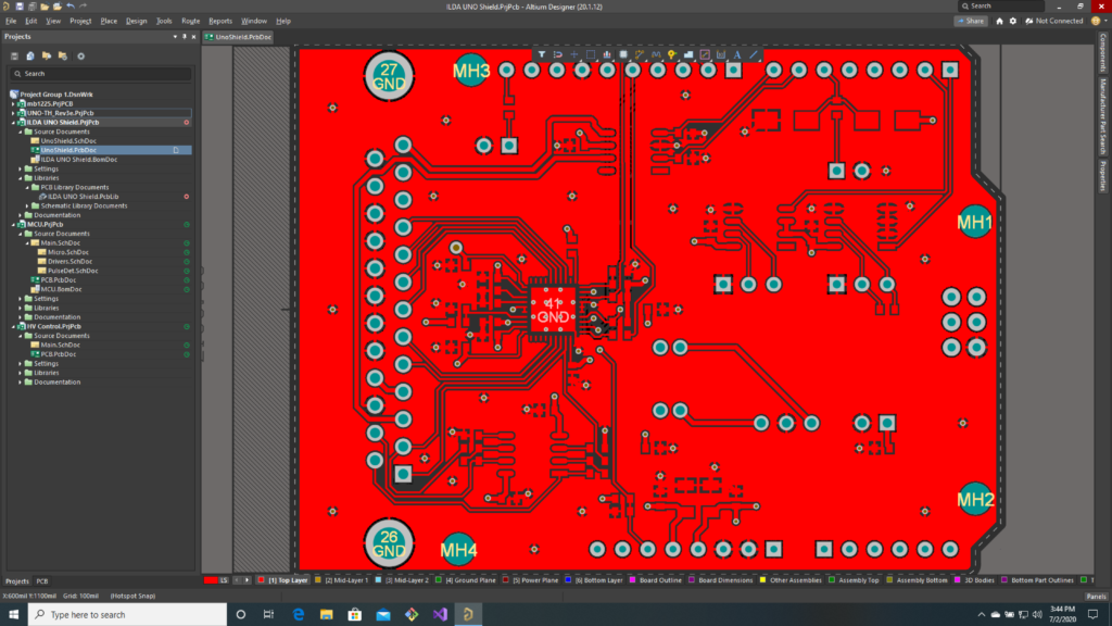
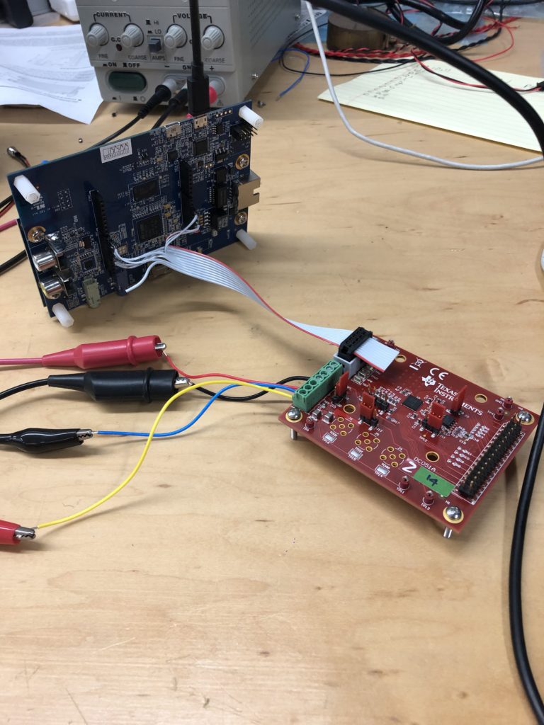
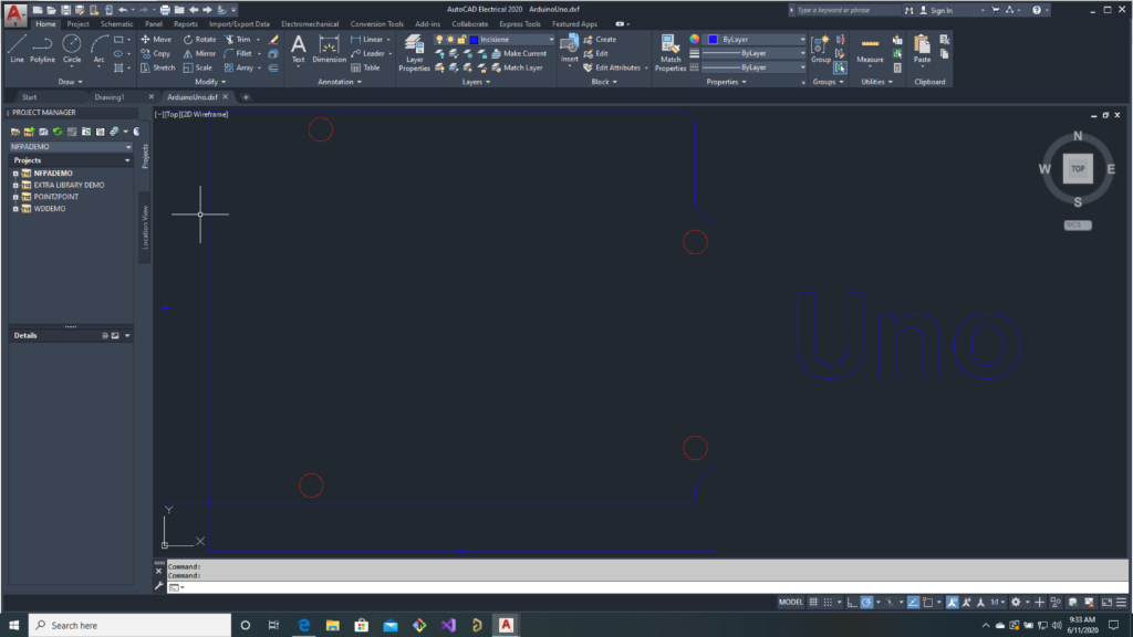
As we say in the last post, our adapter board is pretty simple. So the PCB was quick to route. Most the signal connections on on the top layer:
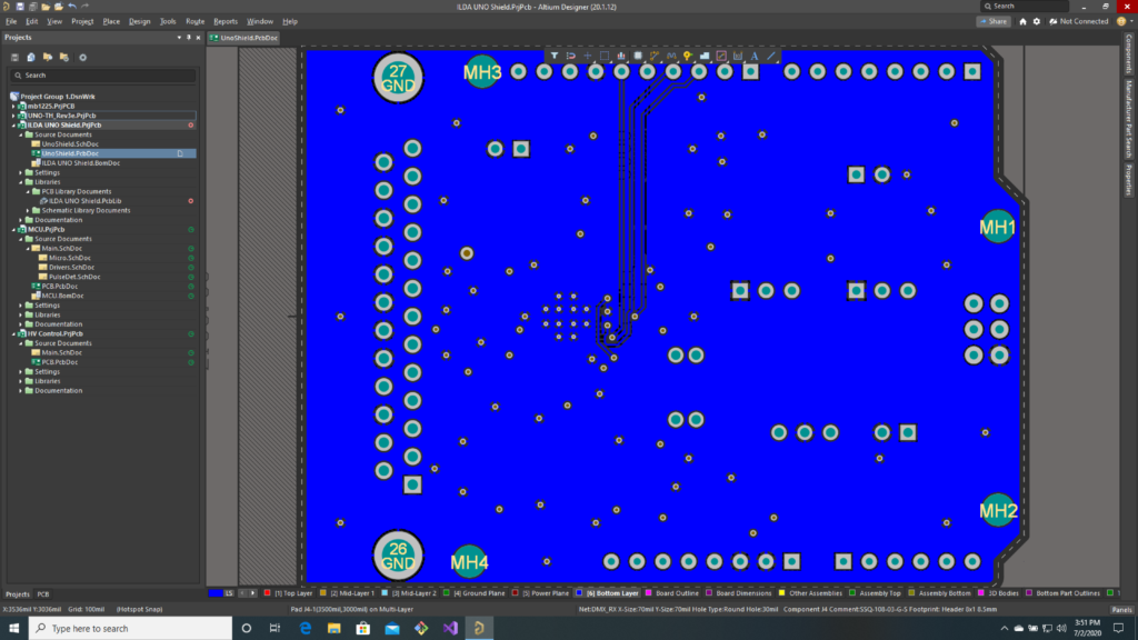
With the SPI signals we use the most (SCLK, MOSI, and NSS) on the back:
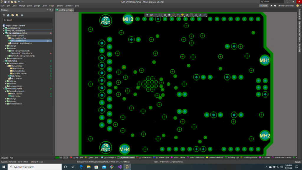
At 25-50 MHz, they are a potential noise source. There is a pretty convention ground plane:
We’ll see what the fabricator’s DFM tool says about all those ground spokes clipped on QFN footprint from TI. Our last layer is a split power plane, with sections for +5V, +9V, -9V, and +3.3V:
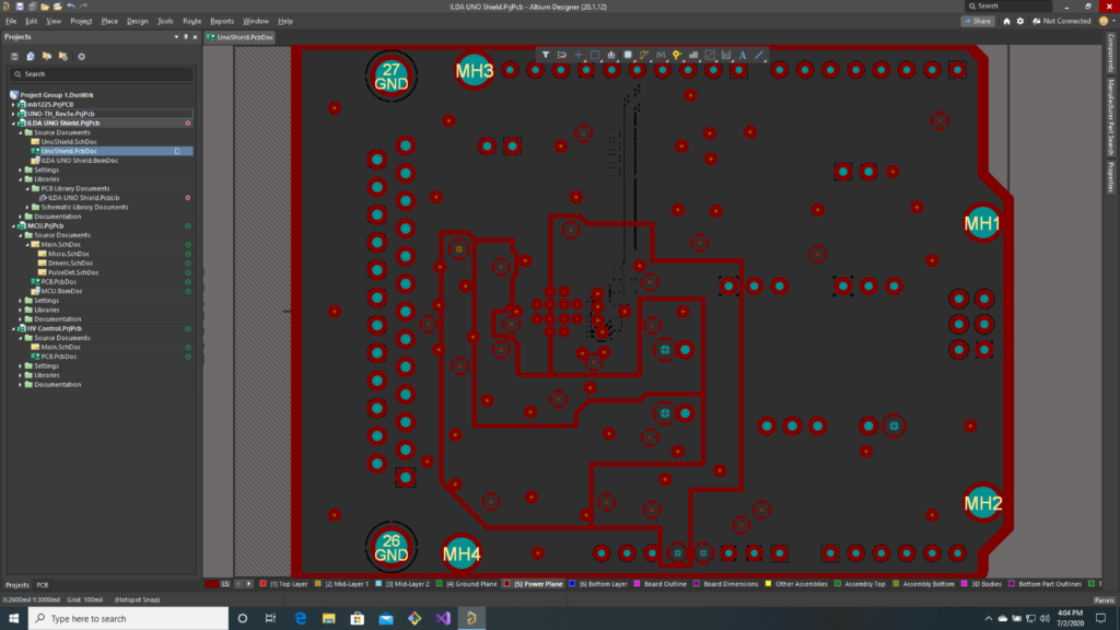
The ILDA projector connection is the big DB-25F at one end. The other connections are on simple .1″ header connectors for now:
Gerbers are generated and submitted for DFM, and everything (Altium design files, library parts, gerber files, etc.) is pushed to the BMC git repo.
Next up, we’ll get a jump start on writing some code while we wait for our prototypes!
Edit: As I feared, the DFM evaluation did not like the footprint for the TI DAC. Internal connections on a PCB generally used “Thermal Reliefs”. The connection is made through little copper spokes so that when the board is being soldered, all the heat does not rapidly transfer to the internal copper planes.
The original footprint had central pad holes that were obliterating most the spokes of other holes nearby, so most of the copper connection was lost. I changed the footprint to an X-pattern:
The board then came back clean:

So I ordered them using the budget special. PCBs should ship back July 13th. I also added a CM (contract manufacturer) quote pack to the git repo. My normal prototype assembler was very reasonable, so I have them setup to do a 1 week turn after boards arrive.
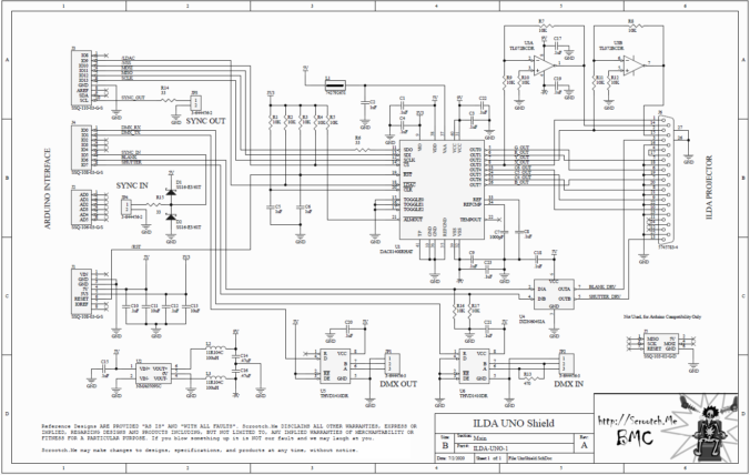
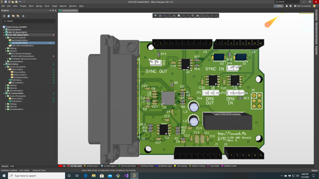
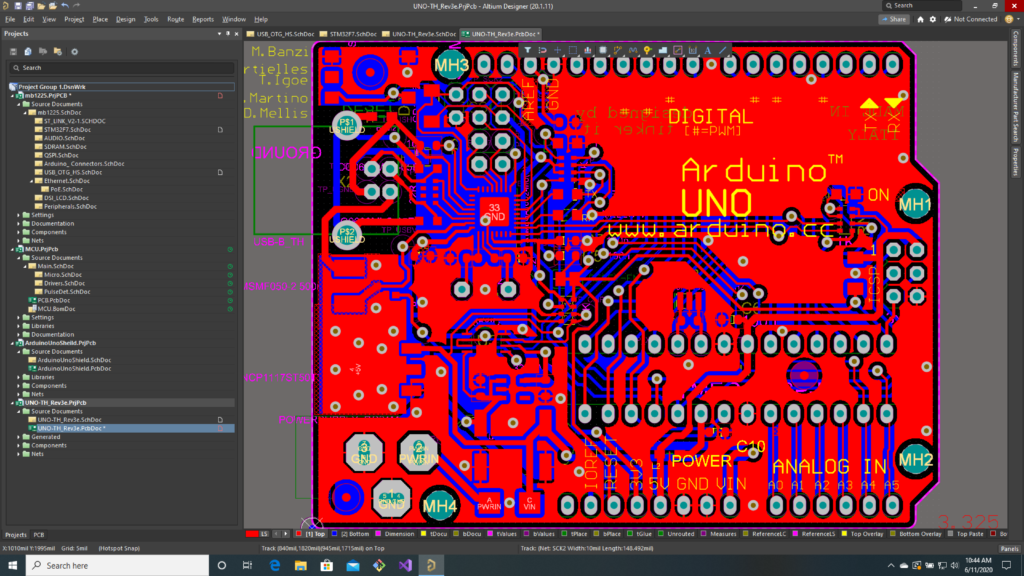
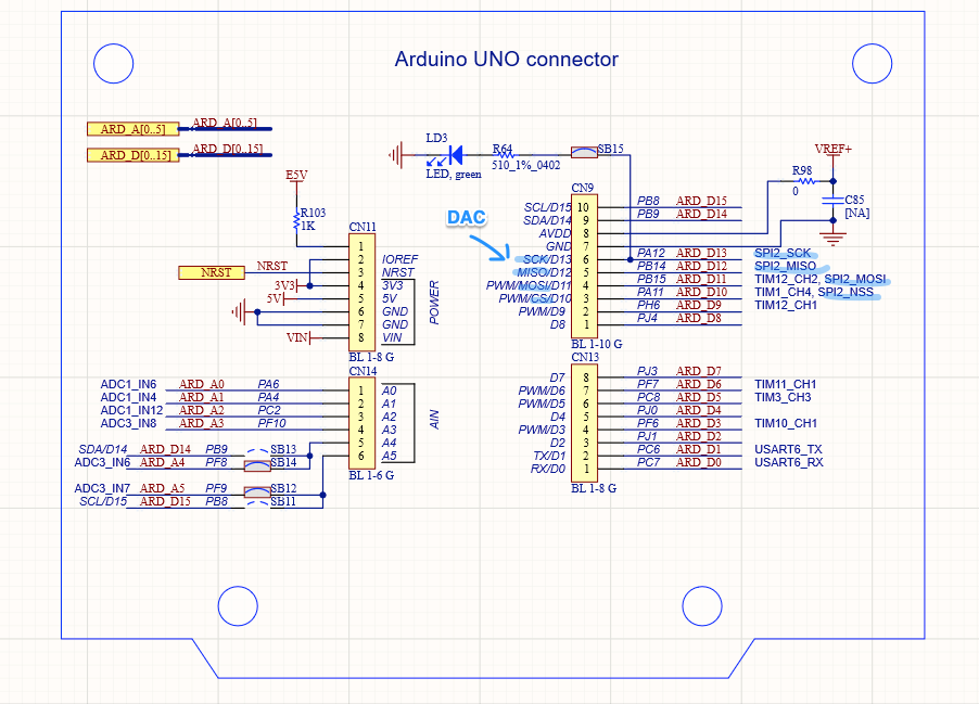
Well, we finally have a schematic for our Arduino UNO compatible ILDA “shield” (PDF version here). It’s pretty close to what we sketched out here. And prototyped here.
A big chunk of the DAC section is just a simplified version of the schematic of the DAC81408 EVM evaluation module we used for prototyping (page 13 here). But there are a few extra sections worth covering briefly.
Power
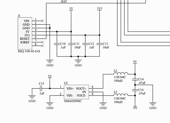
Only 5V and 3.3V come to our board from the host card. In the lower left corner you can see we have some filter caps to clean up the voltages provided and a DC-DC switching converter to provide +/- 9V from 5V in.
We probably could have gotten by with just a 5V to -5V converter, but I was a little concerned that the input impedances of ILDA projectors isn’t really called out in the specification. So I wanted a little extra headroom in case I need to switch op amps to get more drive (more on that below).
Inverting Amplifiers
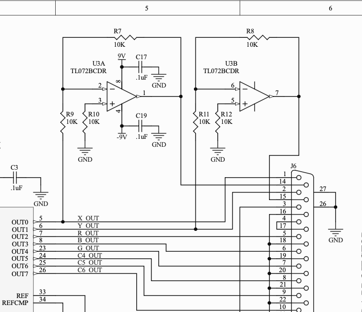
In the top right corner you can see some inverting amplifiers with a gain of 1:1. I used a TL072BCD. It is a common JFET op amp with good harmonic distortion and a fast slew rate. My one concern is that it only has a few milliamps of drive capability. But if this turns out to be a problem the footprint/pinout is common to a number of other amplifiers we can switch in.
If you haven’t worked with op amps, you can download a SPICE model for this one here. LTSpice is a free version of SPICE for Windows that many electrical engineers use. Although it isn’t perfect, simulation is a great way to try things out without prototyping them. In this case, I know that the inverting amplifier will put out an inverted form of the +/-5V signal I put in, but we can still quickly check performance at higher frequencies:
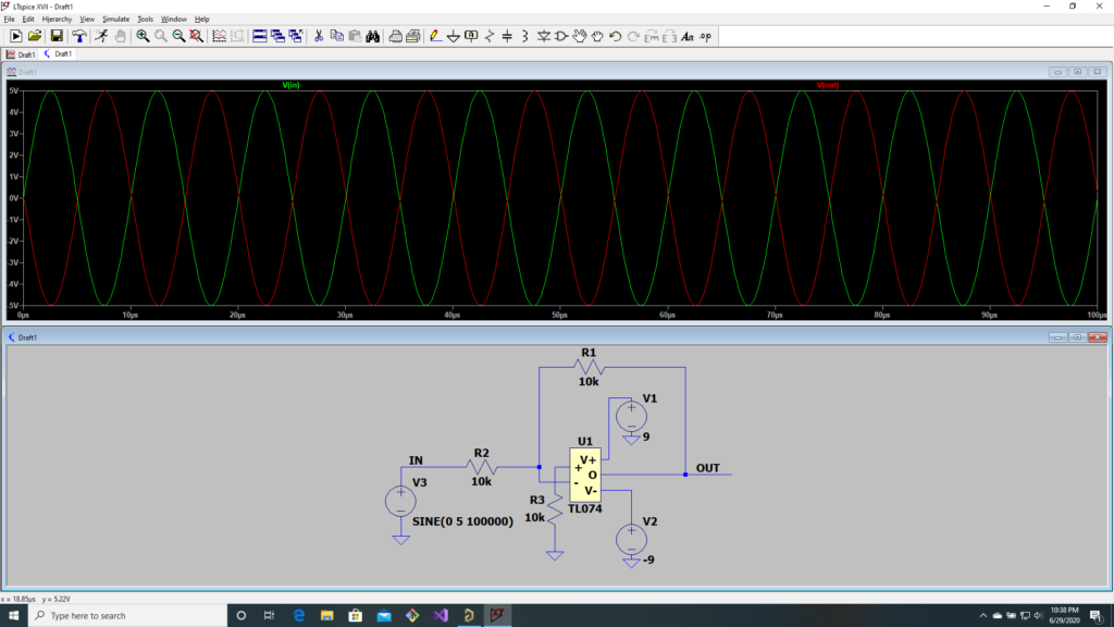
Looks good up to 100 kHz in but, again, my concern is if we have enough output drive capacity for the projector.
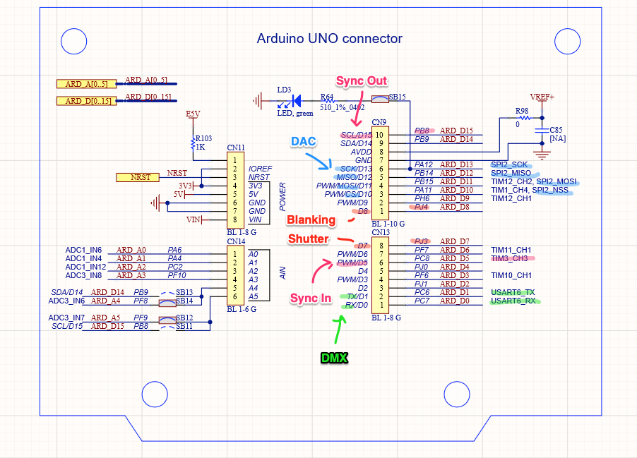
Driver Chip
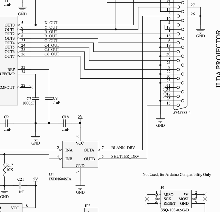
Because a shutter and (possibly) a mechanical intensity control can be inductive loads, there is a two channel driver chip for those signals.
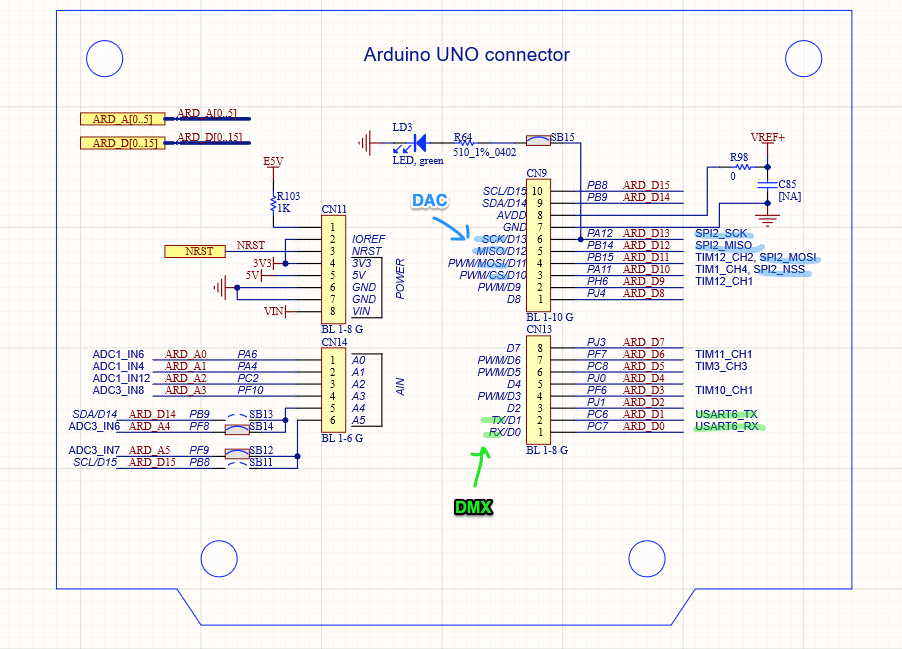
DMX In/Out
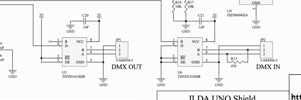
Along the bottom of the schematic is our DMX circuitry. We have a UART controller on the main board, so we only have to provide RS-485 transceivers. These can operate half duplex, but we have one fixed for receiving, the other for transmitting. We also have a termination resistor on our input.
I thought about making our output more sophisticated to support something called Remove Device Management (RDM), but decided to keep the DMX simple for now.
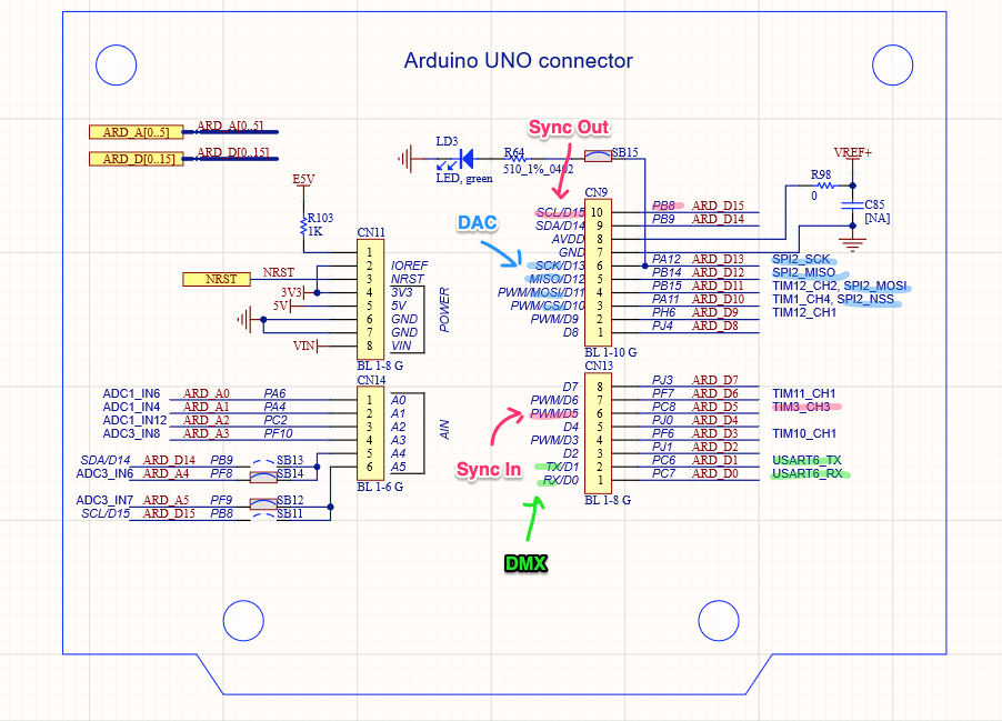
Sync IN and OUT
As planned, Sync In and Out are pretty simple general purpose IO from the MCU. Both just have a pad resistor for ringing and a little bit of current protection and the Sync In has some beefy protection diodes added. These do add some capacitance to our input, but it should be fine for the frequencies we are interested in for now, and the extra protection diodes give some piece of mind.
That’s about it. I’ll push everything to the BCM git repo as soon as I wrap up the first revision of the PCB.
Next stop, gerber files…
In the last post I mentioned that I would be posting the Matlab scripts in a public source repository once I settled on an open source license. I’ve selected Apache 2.0 as the license and setup a git repo here.
I went ahead and added a third script:
function DrawIldaFrame(x, y, z, s, c, showBlanked, view3D, target)
% Plot an IldaFrame
% Inputs:
%     x, y, z, status, and color information
% Optional Inputs:
%     showBlanked (0 or 1) to show blanked points
%     view3D (0 or 1) to show in 3D
%     target axes to plot to
To make it easier to quickly plot an imported ILDA frame. And a simple applet built with Matlab’s App Designer:
It’s a tad slow but, as I promised before, we will be writing something much better down the road. In addition to letting you scroll through all the frames in a file the app does try to honor any color information that is included. But I only tested with a small number of ILDA files so the scripts might need tweaking for some of the allowed file format variations:
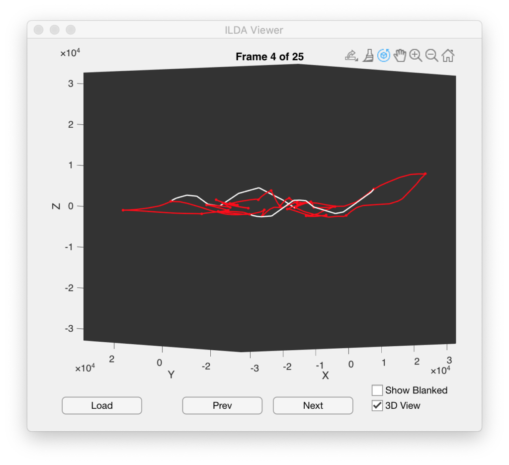
You can also put the Matlab plot in 3D mode to examine graphics that use the Z axis (many don’t):
The standard Matlab popup tools are still there so you can orbit around 3D space, zoom, pan, export views, and etc.
One thing that can be interesting to do is to display the blanked parts of the frames as well:
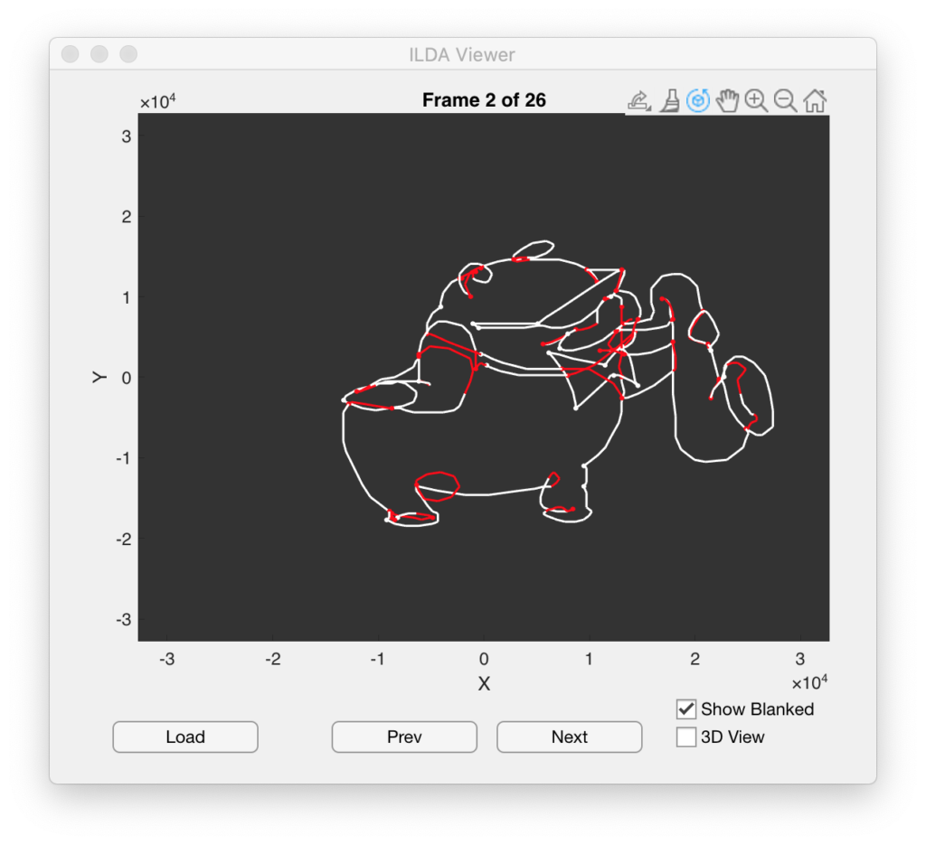
One of the things that keeps striking me is that some of the best looking graphics are still ones that were done 35 years ago on an 8 bit system using slower scanners and mechanical blanking. Because of the limits of the technology back then the artists would do things like turn corners with loops and blank along the imaginary surfaces of the object being draw (like the mouth of the sax above). These techniques stopped visible line ends from bending at less artistic angles and made any imperfect blanking/light leakage look more natural.
Another technique you’ll find is excess blanked points in some animation frames. For example, this bulldog has some large loops of blanked points:
Later in the animation he swells in size:
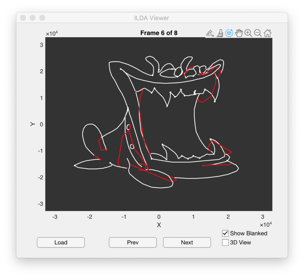
In that frame the excess blanked points in parts of the image are greatly reduced. As we will see later, image manipulation, like position, rotation, etc. should typically only occur after each complete scan of an image. Otherwise the image will look like it is tearing to the people watching it as it moves. Because every frame must typically be drawn in its entirety, keeping the number and distribution of total points fairly even from frame to frame helps animations look smoother and more uniform in brightness.
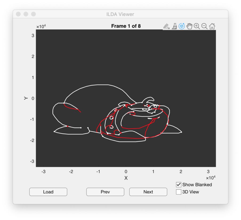
As we can see from looking at newer images, this appears to be largely a dead art form. People tend to move in straight lines from one blanked section to another and do not give much thought to drawing order, or consistency from frame to frame:
That’s about it for this little bit of Matlab/ILDA file housekeeping note. I’ll be back soon with some more on the main aspects of our project!
In the last post we sketched out our basic Arduino Uno compatible “shield” board for ILDA projector control. I then indicated that I would start converting that sketch into a proper schematic next. I did begin that process, but when I work on hardware designs I try to also give some thought to how software/firmware will interact with it.
I have used the TI DAC discussed last time in another project and knew that the speed and output quality were on par with what I wanted, but I didn’t like how the interface with our selected control board was shaping up.
The problem is the implementation of SPI (‘Serial Peripheral Interface’) on each chip. The ST MCU’s onboard SPI controllers are pretty good. You can setup the peripheral to output memory directly via DMA (Direct Memory Access) and there is even hardware support for CRC (Cyclic Redundancy Check) error checking. The Achille’s heel is the ‘NSS’ line. NSS stands for “Negative (Active Low) Slave Select”. Basically, this line signals a slave device when it should receive data.
The ST SPI peripheral can drive the NSS line automatically, but only for packets of either 1 or 2 bytes in length. But the TI DAC I selected uses a 3 byte packet. So we would have to use the NSS line in software controlled mode.
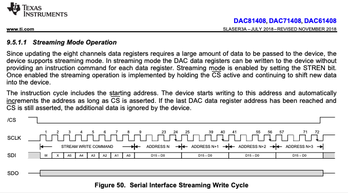
Further, if we look at the operating modes of the TI DAC, the only one really suitable for our purposes is ‘stand alone’:
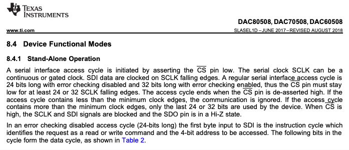
In this mode we have to write to each of the 8 DACs individually and control NSS (connected to the /CS pin on the DAC chip) via software each time. That’s a lot of firmware overhead managing an I/O line just so we can update our DAC values. There are some ways we could work around this with some hardware tweaking, but all the ones that I could think of involved modifying the MCU board to use other peripherals and pins, so I started thinking about DAC alternatives. As it happens, I’ve been working with another TI DAC on a work project, a DAC81408. I even happen to have the TI EVM (Evaluation Module) for it!
But I had two concerns about moving to the DAC81408. First, it is about $15 more expensive in small quantities than the DAC80508. Not the end of the world, but something to keep in mind. Second, the spec’ed settle time is 2.5x longer (12 uS vs 5 uS):
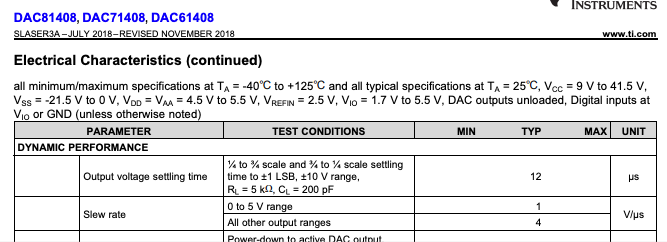
As a rule of thumb, a settle time at least two times faster than your max sample rate is a good starting point. 1 / 0.000005 = 200,000, more than 3x our max sample rate of 60,000. But 1/ 0.000012 = 83,333, just barely 1x our max. But the DAC81408 has some very wide output ranges (ex. +/- 20V) that can be selected, and settle time would be worse on an amplifier at those gains, so it was not clear how the DAC would perform for our application.
Fortunately, the EVM board has just two chips on it, the TI DAC and an external reference chip we aren’t using:
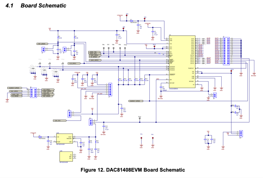
There is also a handy connector for accessing the critical signals we need:
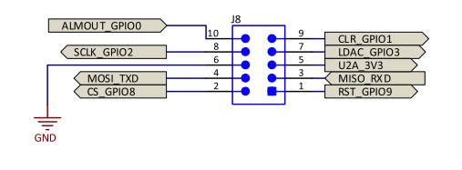
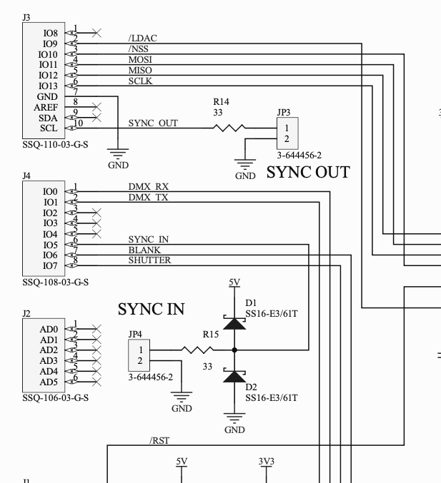
Four of the signals are for SPI and you might recognize them from the last post, but we are going to also make 5 additional connections:
The extra signals are 3.3V and GND from our controller board, the reset signal (NRST) to reset the DAC when our MCU resets, and two additional GPIO lines. These last two aren’t strictly necessary, but they give us access to the /CLR and /LDAC functions. /CLR immediately sets all DACs back to 0V and /LDAC can be used to “Load DACs” with a new value simultaneously. Our test connection looks like this:
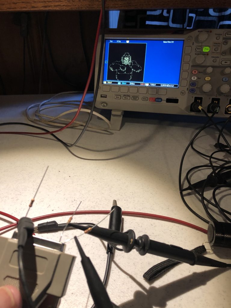
I already had used this DAC for a work project, so getting the SPI communication working with our EVAL board went pretty quickly. I ended up using the DAC in “Streaming Mode”:
This writes all the DAC values in a single SPI transaction, with all the DACs updating when the /CS line goes high again (or, alternately, when we trigger the /LDAC line). Doing all the writes in a single transaction eliminates the wasted firmware overhead. But what about settle time?
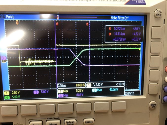
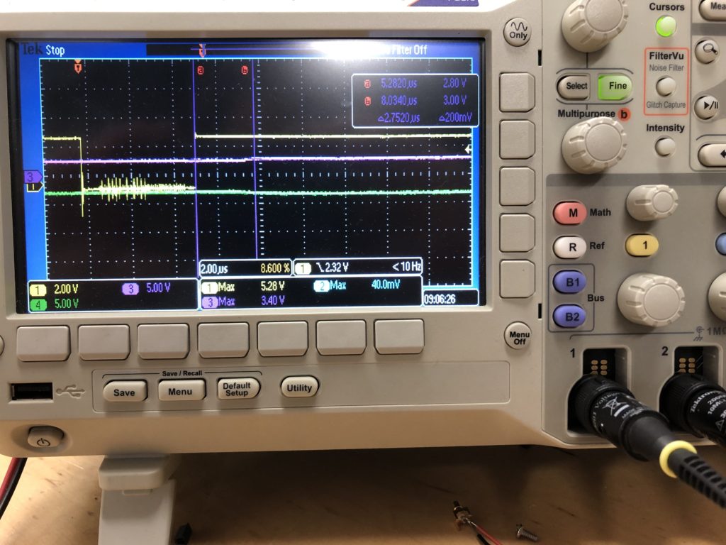
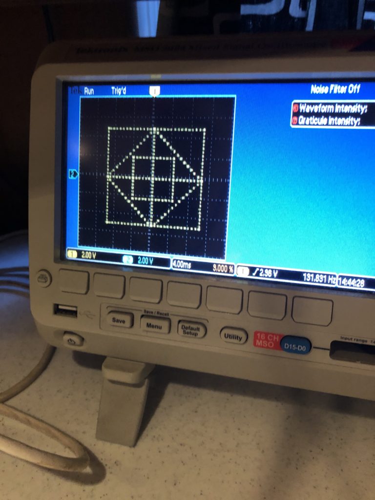
When it doubt, measure it. When operating in the +/-5V range we need for scanning, a full range jump settles in just over 5 uS in both directions (see the scope image at the top of this post). For smaller steps (1/32 of range), it is just under 3 uS:
That’s promising, but the real test is driving actual scanners. You might recall that the ILDA projector spec calls for a “differential signal”, not just X and Y, but X+ and X-, Y+ and Y-. As it happens, this DAC has a differential mode, where a second DAC channel can be set to automatically output the inverse of another. We most likely wouldn’t use this in a final design, since there are much cheaper ways to make a differential output, but it means that we are theoretically just a cable and some programming away from testing the DAC out for real.
This brought up a question of what to scan? Fortunately, ILDA has a specification for exchanging laser graphics. But it appears to be less well supported than one would hope (we’ll save that for a later post). A quick web search turned up a few pages with free-for-non-commercial-use ILDA graphics files, like this one.
With some ILDA files in hand, the next step was to read them and convert the data into something we could quickly put into firmware to test. We’re going to come back to this and write some nice, platform independent code in C++ for managing ILDA files on Mac, Windows, and Linux but, for a quick fix, I wrote two scripts in Matlab.
I wanted these anyway because Matlab already has 3D plotting and is a great platform to test all the matrix math operations that we’ll be adding later. I’ll post the scripts to a git repo in a day or so. I just want to add an “as-is, screw you if it doesn’t work or breaks anything” disclaimer first. [EDIT: More info and a link to the repo can be found here.] Anyway, the two scripts are pretty simple. First:
function [offsets fpath] = FindIldaFrames (inputfile)
% Find the offset of all the ILDA frames in an .ild file
% The inputfile can be omitted and the script will open a file selector
% Outputs a Nx1 matrix of offsets and (optional) the full path of the file parsed 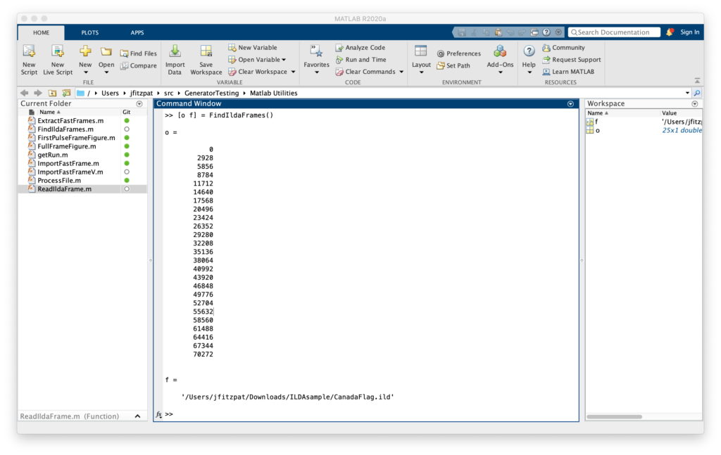
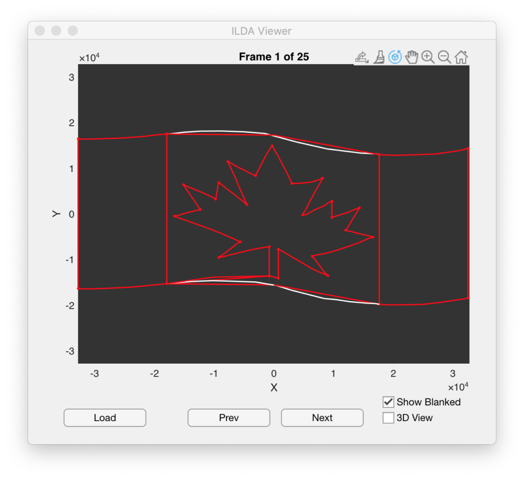
In this case ([o f] = FindIldaFrames()), we got two variables o, with the 25 offsets to frames in the file selected, and f, the full path to the CanadaFlag.ild file parsed (courtesy of function [offsets fpath] = FindIldaFrames (inputfile)). The second script gets the important data:
function [x y z s c] = ReadIldaFrame (inputfile, offset)
% Extract the X, Y, Z, status, and color information from a frame in an ILDA file
% If the inputfile is not provided a file selector dialog will appear
% Outputs the data in Nx1 matrices, except color (c), which can either be
% Nx1 if the file uses color indexes or Nx3 (R G B) if true color is used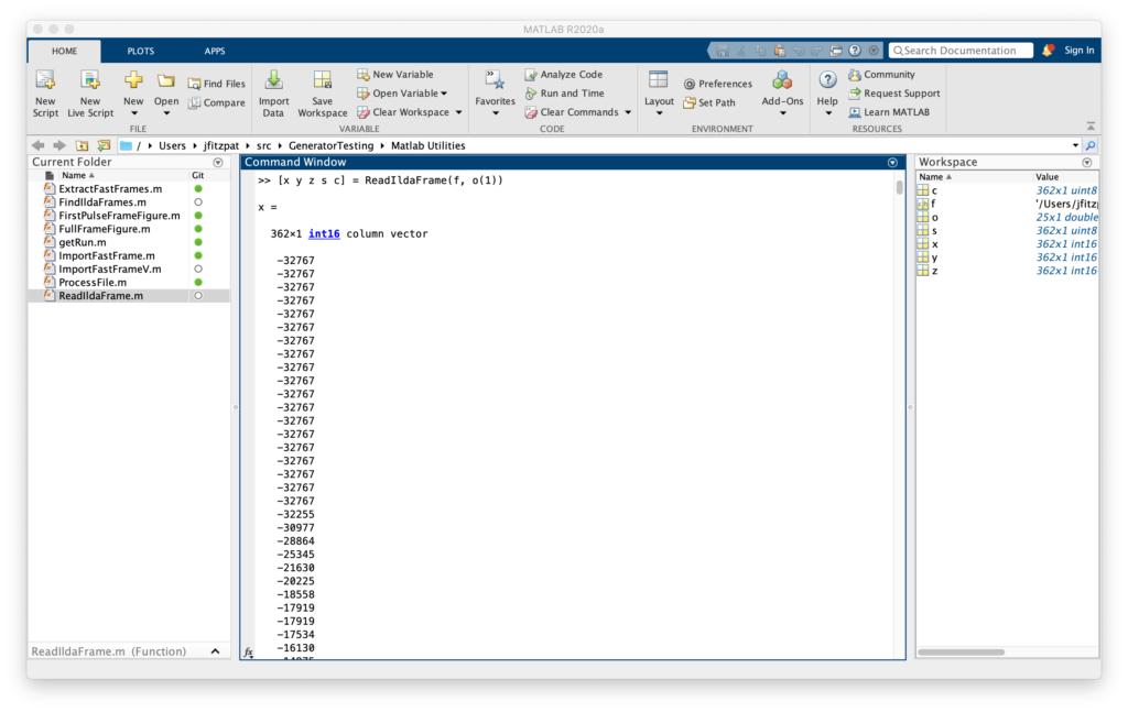
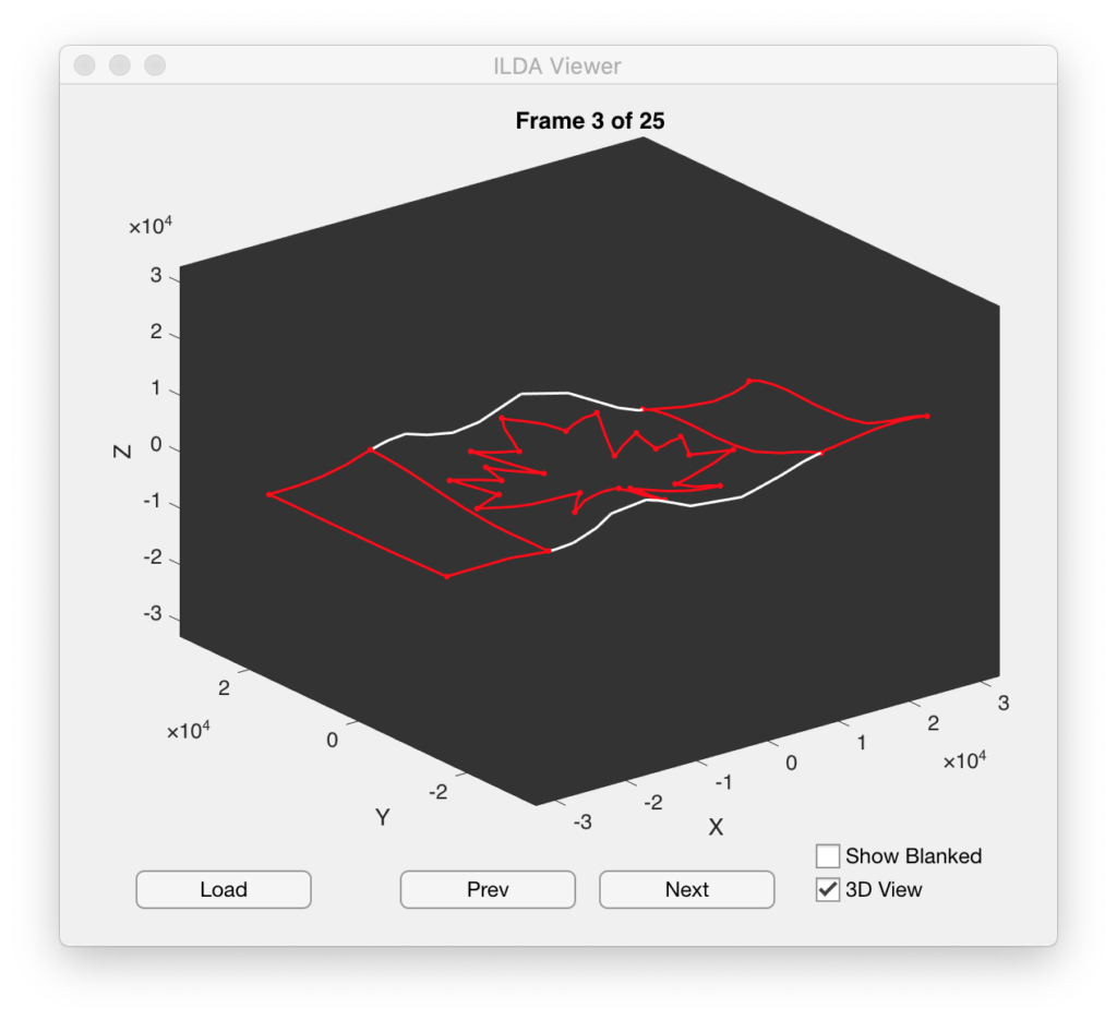
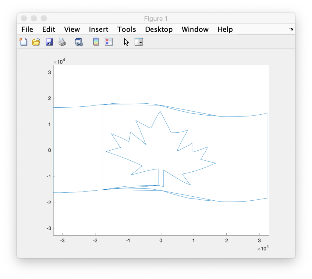
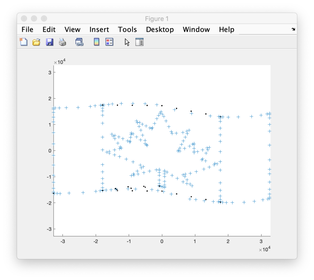
In this case ([x y z s c] = ReadIldaFrame(f, o(1))), got us all the data for the first frame of the file we parsed in the previous operation into some new variables. Entering plot3(x,y,z) will then show us, yep, it’s a Canadian flag drawn in 3D, we can rotate around:
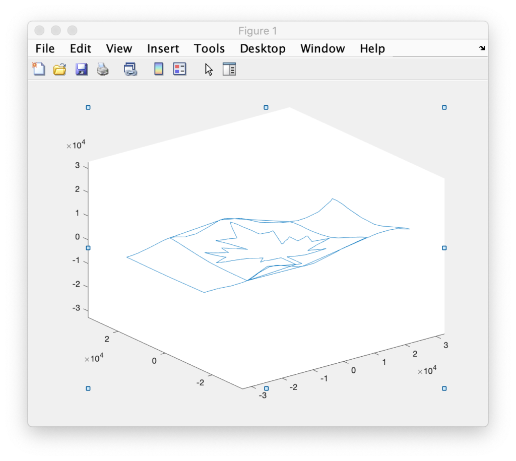
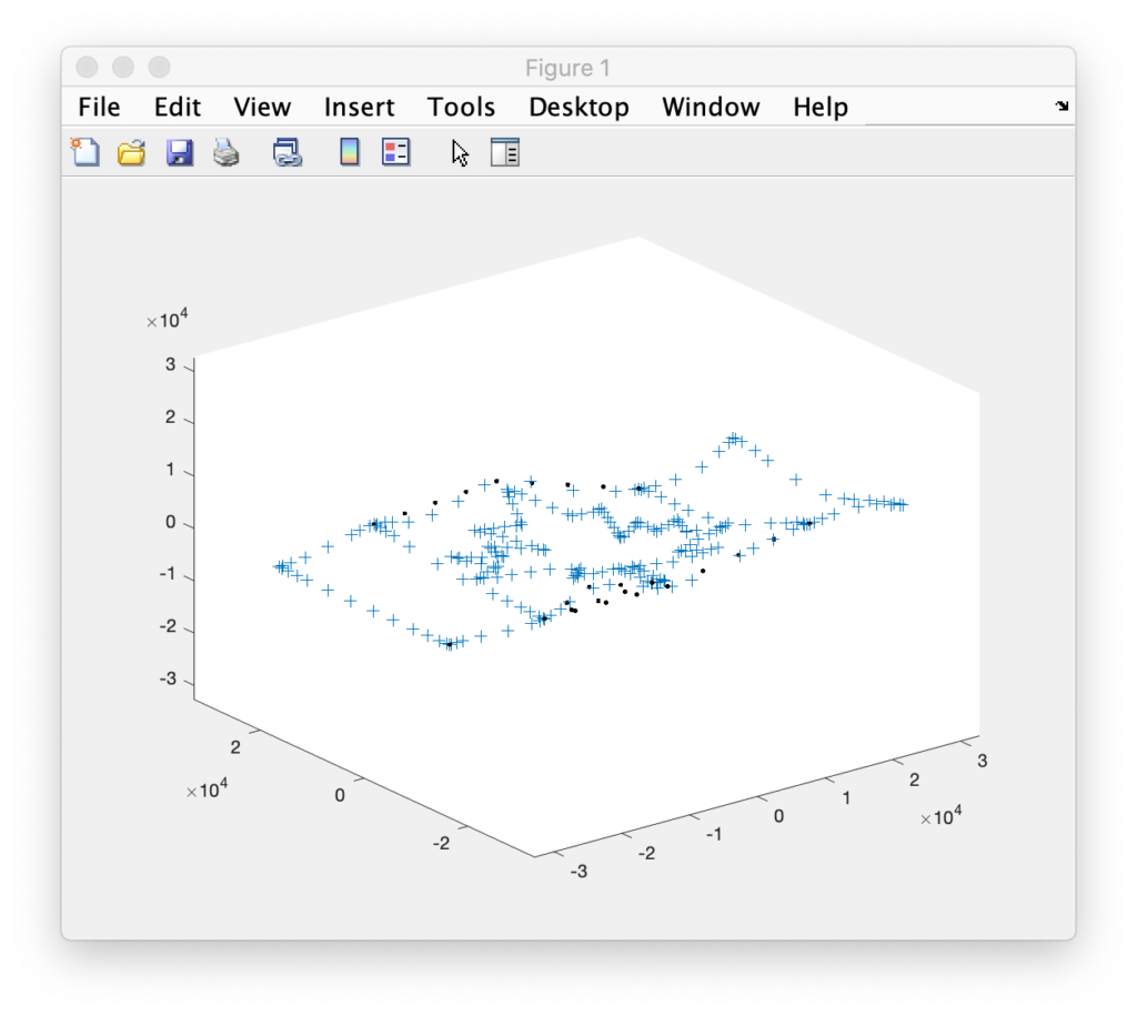
But we are seeing points and connections that are supposed to be ‘blanked’, or invisible. We can quickly distinguish the two using the status data we extracted. The status byte tells us one of two things, if a point is blanked, or if it is the last point in the frame. Entering:
>> blanked = s & 64;
>> visible = ~blanked;
>> plot3(x(visible), y(visible), z(visible));
>> hold on;
>> plot3(x(blanked), y(blanked), z(blanked));
Will plot the blanked and unblanked parts of the frame in different colors. It also can be helpful to change the graph to view everything as dots:
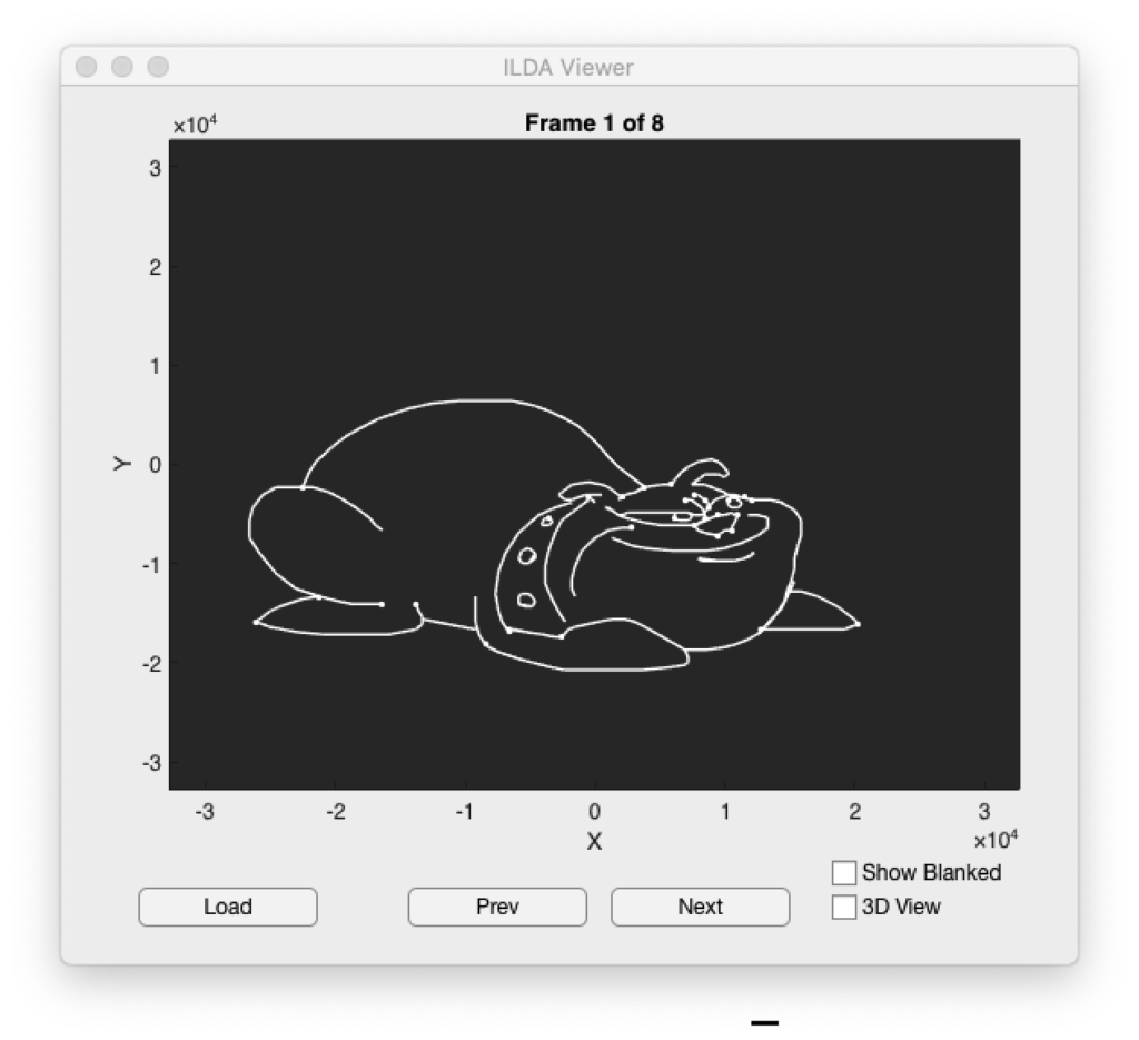
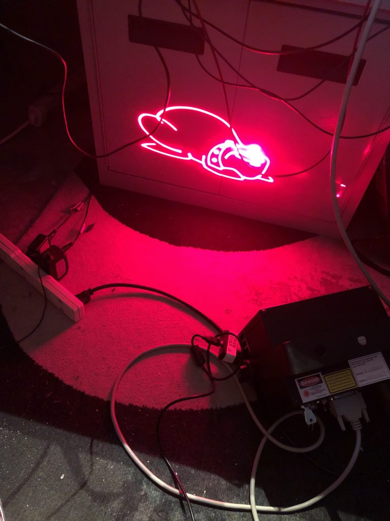
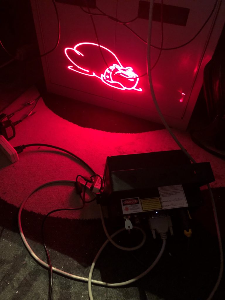
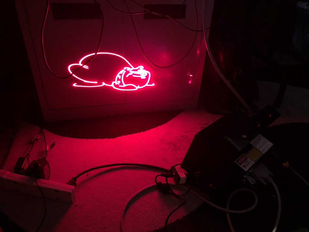
I was all set to do the scan test with a Canadian flag until Marty Canavan at YLS Entertainment sent me some vintage graphics as ILDA files. One of them being good ‘ol BULLDOG!
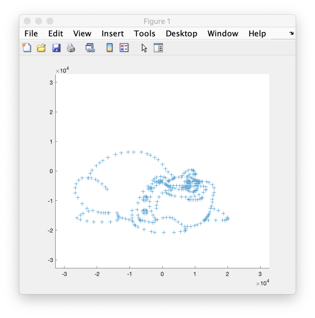
BULLDOG is actually an 8 frame animation, of which this is just one frame. It doesn’t look like much plotted this way, but it has always looked great as a scanned laser image. It was made during LaserMedia’s heyday, when the company employed artists and animators from Disney. They factored in how the scanners behaved in terms of inertia, etc. Alas, I can’t remember the particular artist’s name, but I distinctly remember using this animation when it was brand new. So, of course, it has to be the one!
Getting the data from Matlab to the compiler for our Eval board was easy. I used dlmwrite() to create comma delimited text files with the data and then included them in a C++ source file like this:
const int16_t dogX[] = {
#include "dogX.inc"
};
const int16_t dogY[] = {
#include "dogY.inc"
};
const uint8_t dogS[] = {
#include "dogS.inc"
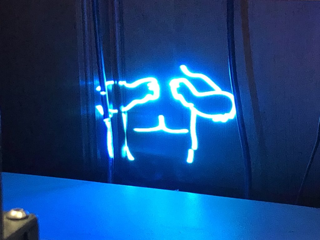
};Putting the image data in flash memory. Z data was all 0s and color data was all white, so I didn’t bother putting them in for this test drive. I setup a timer to scan the data and everything looked good, out to 60 kHz on the oscilloscope:
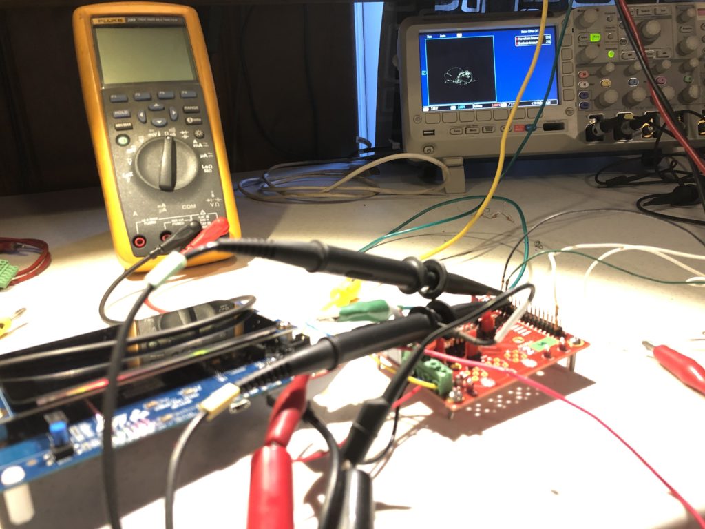
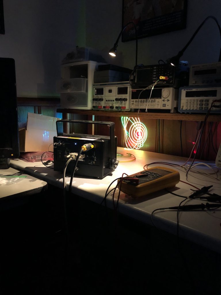
So I threw together a super kludgy DB-25 wire harness (reminiscent of a spider in honor of the lab mascot who came with the loaned projector):
Set the scan rate down to 14 kHz (what the image was originally drawn for), and hooked up the laser projector:
The rolling shutter really messes with our image (we’ll get to that!), but in person BULLDOG still looks great. If you futz with exposure and focus you can usually capture the whole image, but you lose all the details in the eyes, face, etc. that make the graphic so likeable:
One other thing worth pointing out is what happens when you increase scan speed. This projector is rated to 30 kHz. So I scanned the same image at 20 kHz, 25 kHz, and 30 kHz. The image doesn’t really distort, but what is visible and what is invisible shifts:
This is because the diode laser does not turn on and off instantly. We’ll address this down the road.
Next we will be back on our proper schematic and PCB, or maybe not!
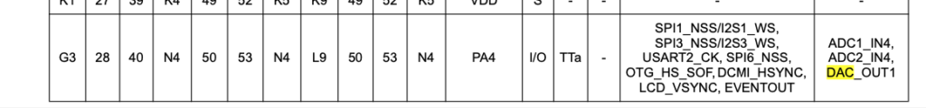
In the last post we settled on a controller card to run the laser projector. But to control XY, color, shutter, and etc. we are going to need some DAC and digital control channels. Based on the ILDA projector specification and our measurements, I believe we will need the following MCU channels:
| Channel | Type | Description | Output |
|---|---|---|---|
| 1 | DAC Output | X | -5~5 |
| 2 | DAC Output | Y | -5~5 |
| 3 | DAC Output | R (C1) | 0~5 |
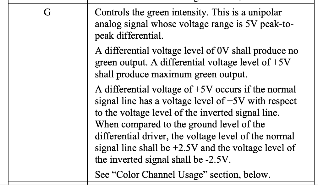
| 4 | DAC Output | G (C2) | 0~5 |
| 5 | DAC Output | B (C3) | 0~5 |
| 6 | DAC Output | C4 | 0~5 |
| 7 | DAC Output | C5 | 0~5 |
| 8 | DAC Output | C6 | 0~5 |
| 9 | Digital Output | Intensity/Blanking | 0/5 |
| 10 | Digital Output | Shutter | 0/5 |
| 11 | Digital Input | DMX RX | 0/5 |
| 12 | Digital Output | DMX TX | 0/5 |
| 13 | Digital Output | Sync Out | 0/5 |
| 14 | Digital Input | Sync Input | 0/5 |
Note, in the ILDA specification a number of these signals are differential. That is, there isn’t just an X signal, but an X+ and X- signal. We’ll address this on our IO board, but that isn’t something that the MCU will be concerned with.
There are also a number of signals that aren’t in the spec and which we haven’t mentioned yet. So let’s review the signal groups one at a time. But first, let’s go over our basic PCB platform.
The PCB and Dev Board Connection
As I mentioned in the last post, our STM32F769 based eval board has a connector for Arduino expansion modules. Arduino is an open source hardware and software company whose microcontroller offerings are generally based on the older Atmel (now Microchip) AVR AtMega processors.
Although I am familiar with the AtMega MCUs, the Arduino DIY world is not something I have any experience in and, frankly, is something I don’t want to invest a lot of my all-too-limited supply of remaining neurons on. Still, if we are going to make an IO board based on a standard, we should at least make a cursory effort to comply. Step one would be the physical footprint and connector locations for our PCB.
For reasons I don’t understand, Arduino expansion cards are called “Shields“. They are supposed to be the same size and shape as the Arduino board itself for stacking. For reasons I suspect I do understand (cough cough, they want to sell you stuff), the hardware specs are a little hard to access. The official Arduino Uno rev3 link does have a tab for technical documents, but there are less useful than you might expect. For example, the DXF drawing of the PCB does not show connector positions:
There is a schematic in PDF form, but that doesn’t help us. Which leaves “Eagle CAD Files”. Eagle is a proprietary EDA (Schematic/PCB design) tool from Autodesk. I don’t blame anyone for using a proprietary EDA tool. The most popular free tool, KiCAD, is a time wasting sink hole of frustration. The problem I have with Eagle is that it isn’t a tool I own or use. I use Altium Designer, which is pretty much the industry standard these days.
Altium does have an import function that supposedly handles Eagle files, but the Altium manual pages for the function give a bunch of warnings about what will and will not import correctly. So I was little bit nervous when I launched it and input the two files from Arduino but the results were better than I expected:

The schematic looked pretty close to the PDF version and, while silkscreens and other text were whack, the basic copper and drill areas of the PCB looked reasonably correct. ST lets you download the PCB gerber files for the dev board we are using, so I lined those up with the imported Arduino board to make sure everything aligned correctly:
I was just about to go through the somewhat tedious process of putting together a new board based on the dimensions and part placement of the imported Arduino board when I found that someone had already done this and posted the files on the Arduino online forums. I pulled that project and checked it against the pinout and gerbers and, again, everything looked fine:
Well done guest user “samarkh”! With our board shape, connector placement, and connector pinout handled, it is time to start looking at our channels. First up, the most critical channels for our ILDA projector.
DAC Channels
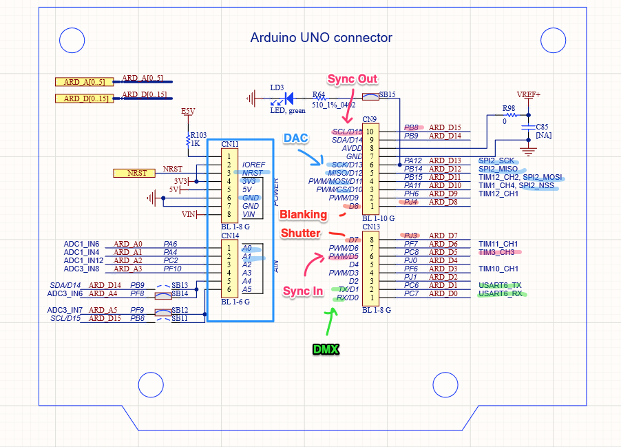
Our first 8 channels are the real core of our laser controller. X/Y position for our scanners and up to 6 channels of color control. The STM32F769 MCU on our control card does have two built in DACs. They are 12 bit (4096 steps) and not horrible, but they are only available on two specific processor pins:
One of those pins does already go to the Arduino expansion connector (PA4 is wired to Arduino A1), but the other, PA5, is used for USB OTG on the board (ULPI CLKOUT):

We are going to want to use that USB connection and 12 bits is a bit lower resolution than I want anyway, so let’s just make our IO board self contained. We can use this 8 channel, 16-bit, SPI controlled DAC from TI.
If we look at the datasheet, we can see that data is output to it serially:
That is, data is clocked to it one bit at a time. If we want to both read and write to the chip the interface is 4 wires (SCLK, SDI, SDO, and CS). If we check the schematic for our eval board we can see that not only are those lines listed on specific Arduino connector pins, they are routed to pins on our processor that can be used for SPI with a built in support peripheral:
If we dig deeper we can see that this setup isn’t perfect. This particular DAC does not offer bulk writing. That is, you can only write to one channel at a time. And the SPI peripheral available, SPI2, is on the slower peripheral bus inside the MCU (see the diagram below), so we will only be able to write to it at 25 MHz, not the 50 MHz it is capable of, but this should still be pretty workable.
This brings up an important point: not all pins on the expansion connector are equal. Some are mapped to pins that can be used with specific peripherals built into the MCU. So I am going to jump out of order a bit and take care of some peripheral specific control channels next.
DMX In and Out
DMX is a standard for controlling theatrical lighting fixtures. It’s clunky and weird with glaring deficiencies (no error checking for packets? wtf!!!) so, of course, it is widely adopted. Basic DMX is unidirectional. Communication only flows in one direction. We will want both a DMX input (DMX RX) so we can be controlled by lighting consoles and a DMX output (DMX TX) so we can control DMX devices. We want this because DMX is often used in laser projectors for beam actuators and motorized effects.
Beneath the DMX protocol is an older serial communication protocol called RS-485. To receive and transmit this protocol you really, really, really want to use a UART (universal asynchronous receiver transmitter) peripheral inside your processor. This is not something you want to do with software and a general purpose IO chip! Trust me, I’ve had to. Thankfully there is a pair of UART pins on the Arduino expansion connectors, so we know where our DMX signals have to be routed! We’ll put RS-485 transceiver chips on our board:
Sync In and Out
We haven’t really mentioned sync signals before, but we are going to want them. For a typical entertainment application a host computer might be monitoring, say, SMPTE Timecode, and sending trigger signals out to equipment over something like DMX, which is often sending packets at about 40 Hz. This is generally responsive enough for things to look synchronized for an audience, but our first gag is going to be to synchronizing our laser projector with a video camera. In that case we want any link to be much more precisely bound.
Obviously, tying signals directly to the processor doing the scanning will make things more tightly synced than two processors talking over a serial link that is only refreshing 40 times a second. But we want things really tight.
Peripherals typically signal an MCU by generating something called an ‘interrupt’ – stop what you are doing and pay attention to me now. IO pins on most MCU’s can be set to do this as well. We could have our sync in trigger an interrupt. But the response time to an interrupt ‘jitters’. Depending on what the MCU is doing when the interrupt occurs, responding to the interrupt will take varying amounts of time.
That may not be good enough for our purposes, so we are going to connect our sync lines to pins that can be mapped to timer peripherals inside the MCU. You might have noticed that a number the pins are labelled with a specific timer and channel. Channel doesn’t really matter. On our MCU, any timer channel can generally be used as either an input or an output to the timer. But Timer number is another matter. If we look at the datasheet for our MCU I linked to in the last post, we will find this very useful diagram:

If we read the documentation further we will find that the timers are:
- One of different types (“advanced, general purpose, and basic”)
- Reside on either a 54 MHz or 108 MHz peripheral bus
- Only can be synchronized in certain combinations
That last bullet point is key. Based on the notes on ST’s schematic, we basically have 4 timers readily available to us, TIM3, TIM10, TIM11, and TIM12. Timers 10 and 11 look tempting, because they are on the faster peripheral bus (and can actually clock at twice that bus speed), but those timers have almost no synchronization options for use with other timers. Not what we want.
TIM3 is the most flexible in terms of triggering and being triggered by other timers, so we will make it our Sync In. TIM12 can at least be triggered by several of the other timers, so that seems like our only choice for Sync Out, but it is kind of sucky so… we’ll double check the docs instead of just trusting someone’s notes on a schematic!
According the the STM32F7xx datasheet, pins PB8 and PB9 also can be mapped to TIM4, a timer with good synchronization options:

Cool! We will use PB8/TIM4 for our Sync Out:
Shutter and Blanking
Finally, some good old fashioned simple I/O. Our shutter is open or closed and the blanking signal is visible or not. We will just map these to some general purpose I/O pins, though we will want to put a driver chip on our board so our MCU pins aren’t hooked to a long cable:
Now that we have a rough design sketched out, our next step will be to make a proper schematic and PCB!
In the last post we met an ILDA laser projector and got a glimpse of the rolling shutter/scanning image problem we are looking to address. Now we need to put together a controller to drive the projector.
When I last worked on laser control 35 years ago the system used a Zilog Z80 CPU running at 4 MHz. The scan rate was about 14 kHz (70 uS per XY coordinate). If you check the processor manual from Zilog you will see that an instruction fetch took 4 clock cycles, so there were only 70 instruction fetches per coordinate pair available.
With only 70 instruction fetches available a big chunk of available CPU time was spent just getting each new XY coordinate pair from EPROM memory (memory chips with little windows we would erase with UV light) and out to DACs (Digital to Analog Converters). When you consider that the Z80 had no hardware multiplication built in (multiplication was done by repeatedly adding), and the obvious question is, how did the system rotate images around the X, Y, and Z axes in real time?
The secret ingredient was a card with 16 “multiplying DACs”. In a sense, all DACs are multiplying. They have a reference voltage and you input a digital value that causes some fraction of that reference voltage to be output. Essentially, you can think of the DAC as multiplying the reference voltage by a value from 0 to 1.0.
But Multiplying DACs are constructed so that their voltage references can be adjusted over a wide range, including 0V. So the output of one DAC can be fed to the reference of another. Let’s see how this might work for something simple like controlling image size.
First, we’ll start with a connect-the-dots fox:
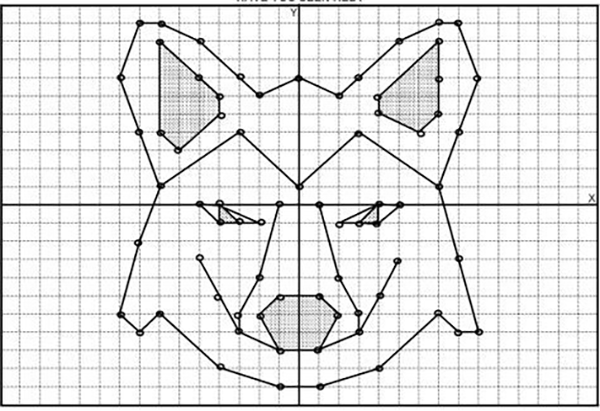
To make him bigger or smaller, we need to adjust all the dots by some scale. If we make the center of the graph 0, 0, the tip of his ear on the right is at 8x, 10y (8 ticks right from center on the X axis, 10 ticks up from center on the Y axis) and the bottom left of his face is -9x, -6y (9 ticks left of center on the X axis, 6 ticks down from center on the Y axis).
Scaling these coordinate is simple. We just multiply. For a scale of 1.0, we get the original coordinates.
[8, 10] x 1 = [8, 10]
[-9, -6] x 1 = [-9, -6]
To scale down to half size, we can multiply by 0.5.
[8, 10] x 0.5 = [4, 5]
[-9, -6] x 0.5 = [-4.5, -3]
To scale up to double size, we could multiply by 2.0. To invert the image on both axes we could multiply by -1.0. As I said, simple but, again, CPU power used to be very limited. So let’s see how we might solve scaling with 3 multiplying DACs:
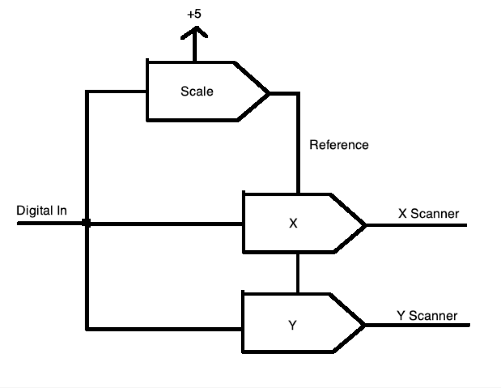
In this case we write our desired size to the scale multiplying DAC once. Then write unaltered X and Y values to their respective DAC channels. The scale channel will alter the reference for the two other DACs from 0 to 5V. Our X and Y values then become a percentage, or scale, of that reference.
This same concept can be extended to a Rotation Matrix, which uses multiplication and addition to move points in Euclidean space, but we’ll cover those in detail in a later post .
For now, let’s just be thankful that CPU power has become a lot more plentiful! We are looking to do something pretty generic and reusable, so I am going to start with an ARM core processor. ARM cores are exceedingly popular and offered by many different MCU manufacturers, so we’ll have lots of choices moving forward. Because of ARM’s popularity, the free tools are also pretty well developed.
There are lots of good choices, but I’m going with an offering from ST. I’ve used a number of different ARM families from different companies, and almost any of them would work fine, but I like some of the MCU peripherals, particularly timers, in the STM32Fxxx family parts quite a bit and, again, ST is pretty well supported by the free tools.
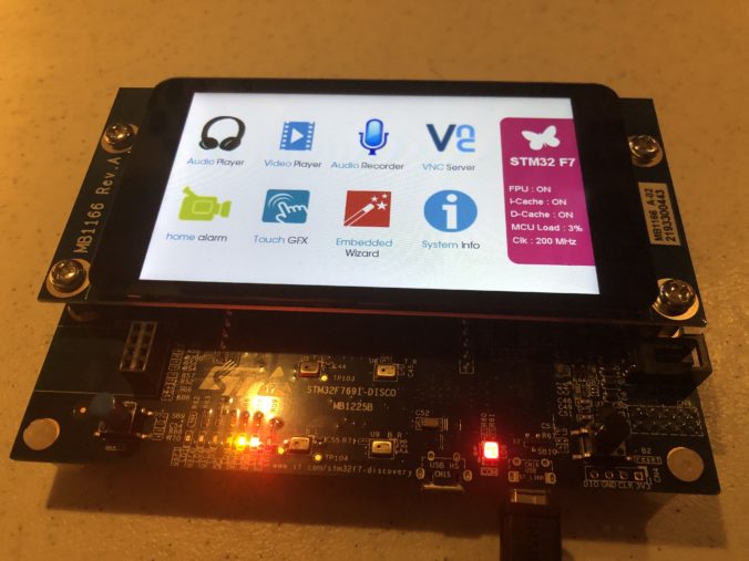
Instead of building a board from scratch, let’s just go with a development board. I’ve selected this one, which is also pictured at the top of this post. It’s got pretty much all the basic IO we might want, like Ethernet, a USB connection, a micro-SD card slot, and a spiffy little color display with a touch screen on it – all for $89. You can also buy the same card without the display for $49.
The MCU runs at 200 MHz, which probably sounds slow by today’s standards, but it is actually more than 50x faster than our Z80 above. The MCU has a faster instruction pipeline, so even if we scan at 60 kHz, we have about 3,300 cycles available to process each point. Further, the part contains both a hardware double precision FPU (floating point unit) and supports something called the “ARM DSP Instructions“, basically 16 an 32 bit integer multiplies and adds in a single cycle.
Some other nice feature are that it has ARDUINO compatible expansion connectors on the back for us to add our ILDA interface support:
And it has a built in programmer/debugger, called ST-Link, so we don’t have to buy an additional JTAG interface to do development (well, yes, I already have a SEEGER J-Link for work, but you might not, and they are a few hundred bucks).
Speaking of development, most the sample code from ST comes setup for the Keil and IAR ARM compiler environments. As it happens, I have access to both of these, but since this is all open source, we’ll stick with the free GNU GCC ARM compiler.
Debugging from a terminal window is doable, but a massive pain, so let’s cobble together an IDE environment for the GCC toolchain using Eclipse. It’s not a great IDE, but its free. In addition to the toolchain above and our IDE, we’ll need a way to connect the GCC debugger to our ST-Link debugging probe built in to the eval board. For that we can use OpenOCD.
It is certainly possible to pull all these pieces together and make them work via primal screams and trial and error, but a somewhat integrated set of instructions can be found here:
https://gnu-mcu-eclipse.github.io/
This project contains some additional CDT plug-in’s for Eclipse that I’ve never really used, but also some project templates for STM32Fxxx based processors and boards that are very handy, not just for getting a base project setup, but also for linking in some of the ST peripheral support library code.
I just setup everyone on OS X, because I like working in it better, but there is no reason you couldn’t setup to build under Windows.
Above I took the basic ‘blinky’ skeleton, modified it so it was on the right IO pin for an LED on the eval board, and turned on and tested the FPU. If you would like to play with the board and MCU yourself, two critical documents are the MCU datasheet and the reference manual. Both of which can be found here.
ST Micro also has a pretty extensive collection of sample code and applications for the processor family and this specific eval board on GitHub.
[Edit] Don’t bother with the GitHub versions. For various licensing reasons parts are excluded and some of the main samples won’t build. You have to fill out a registration and agree to a different license agreement, but get the code directly from st.com.
Next up, we’ll need to start adding some IO!
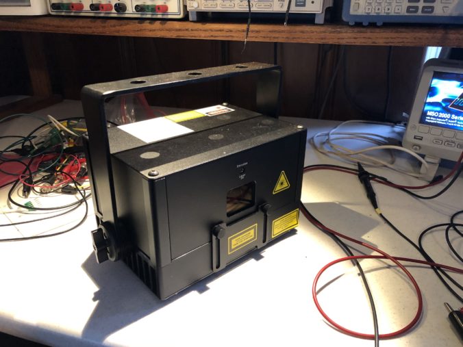
Thanks to Marty Canavan from YLS Entertainment, I now have a borrowed, albeit small, modern laser projector. One thing that has definitely changed from my time in the laser penalty box 35 years ago is the lasers themselves. This little guy puts out several watts of red, green, and blue laser light while being air cooled and running on wall 120V.
In the bad old days, lasers that put out a few watts of white light would be a 4′ water cooled glass vacuum tube with krypton gas, a big electromagnet, and a 560V transformer hooked to three phase power. But enough Grandpa Simpson venting! Let’s get this puppy working.
The back panel seems pretty busy, but the only three things we’ll worry about now are power in – which is 120V, the on-off key-switch, and the connector labelled “ILDA DB25M IN”.
ILDA stands for “International Laser Display Association“. It is a trade group that was getting started just as I left the industry. They publish a number of standards, including one for the projector connector above, which is here.
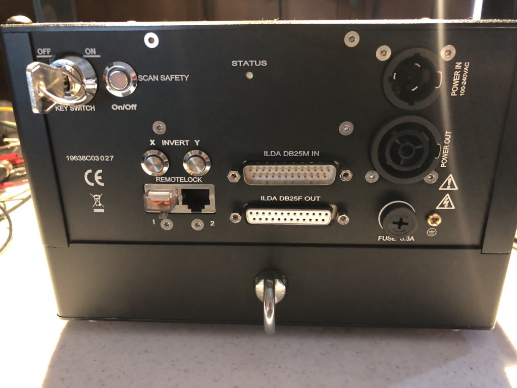
Since the standard is from 1999 and the industry is small, I always like to double check the standard against actual industry practices, so YLS also loaned me an existing scanning system. Alas, I ran into a few hiccups getting it going.
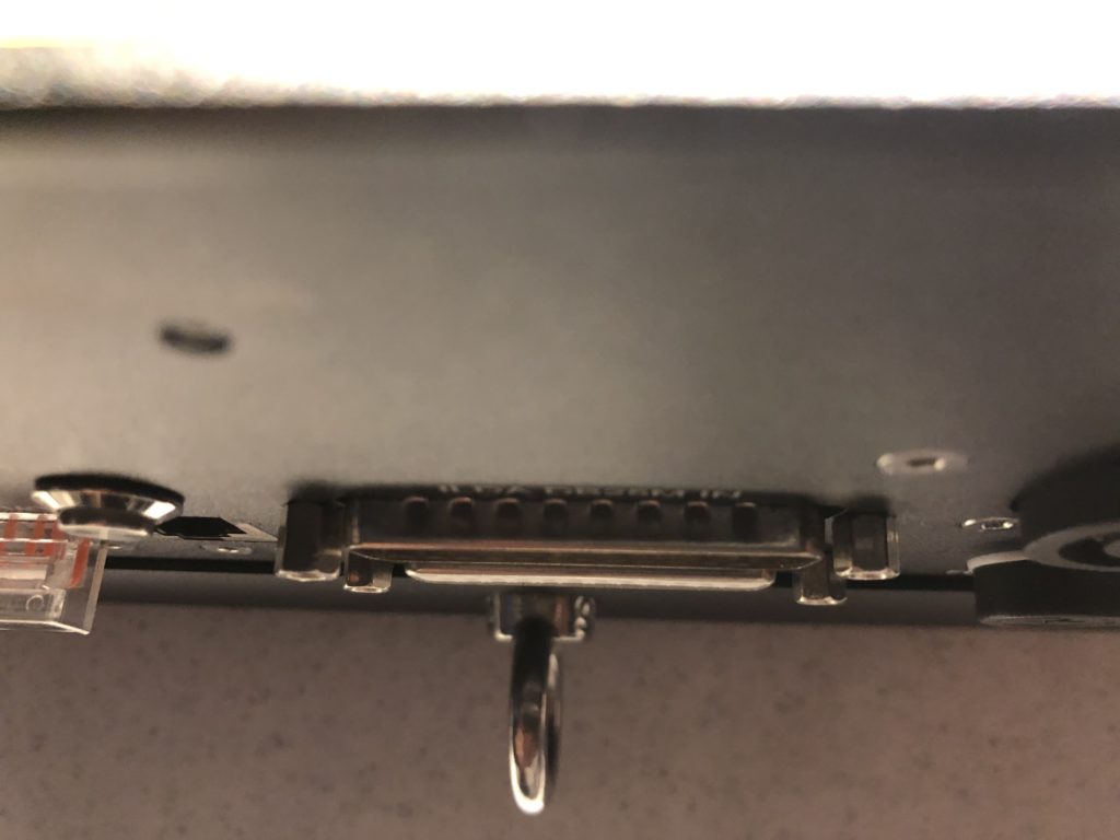
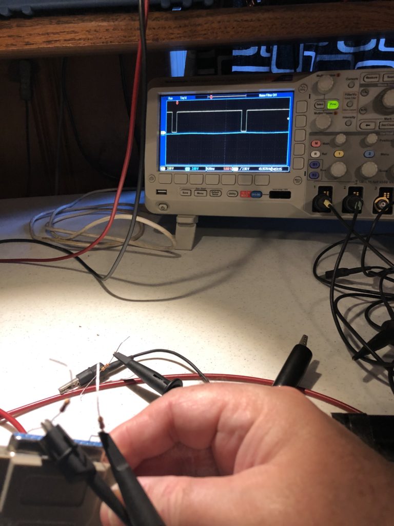
First, the DB25 connector did not fit correctly, so not all control signals were reaching the projector. It turned out that the small DB connector threaded standoffs were not all the same height:
Once I fixed that I had to reach a negotiated settlement with the spider who had taken up residence on the yoke (something tells me this piece of equipment hasn’t been seeing a lot of field time):
With the connector fixed and my new lab mascot settled in, I was finally making bright squiggles!
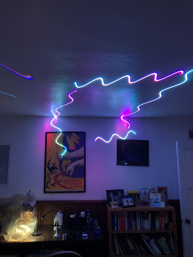
So turned the projector around and started examining signals with an oscilloscope. The X and Y signals were exactly as specified. A 10V differential signal, with the + and – signals both going +5V to -5V relative to signal ground:
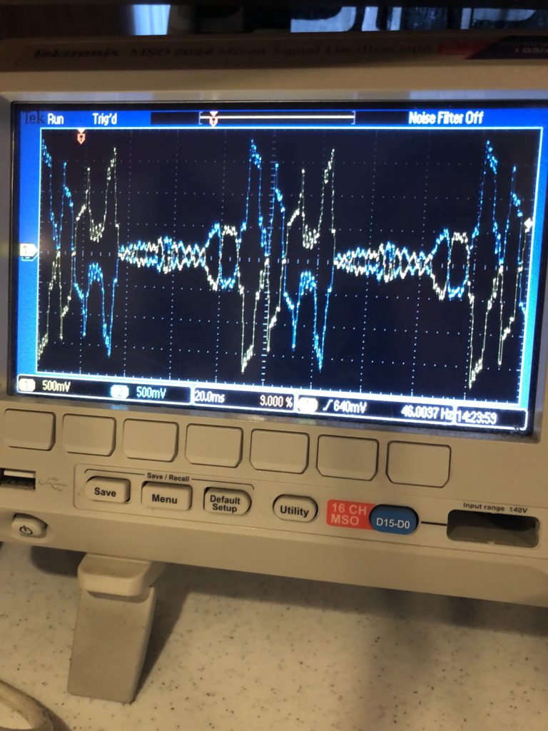
Intensity/Blanking, Shutter, and the Interlock Pins were also all exactly as specified. The only surprise was the color channels. The specification calls out a 5V differential signal with the + and – signals outputting a +/- 2.5V bipolar signal relative to signal ground:
However, there was no deflection on the R-, G-, or B- signals and the R+, G+, and B+ signals all adjusted from 0 to 5V DC relative to ground:
This is still a 5V differential, but does not honor the bipolar properties called out for in the specification. I used a multimeter set to resistance to check for continuity between the negative color inputs and signal ground and it seemed clear that the projector is using a differential input circuit, so I tested a color signal by feeding in +2.5V and -2.5V to the R differential pair and it appeared to work fine.
With things up and running and and the signals all confirmed, I took a quick at the scanning/camera problem I am trying to solve. The oscilloscope has something called ‘persistence’. Traced lines linger awhile, so when we take a photo with a rolling shutter, we get the whole image, but when photograph the scanning laser beam, we only get a part of the image:
This could make for some interesting effects with projected geometrics, but with the existing scanning system tested, the control over image scan rate is too course and the scans themselves are not stable enough. That is, you can’t dial in the exact speed you need and the system doesn’t hold speed consistent enough to get the desired effect.
So, next up, we are going to have to start putting together a control system!
For BMC the straw that broke the camel’s back and got me to work on a new graphic/show control system was requests for help from long time friends still working in entertainment. The first problem I was asked to help solve involves laser graphics and modern video cameras. To understand the problem, let’s first look at the two technologies involved. Laser entertainment projection systems use “vector graphics”. Think Atari Battlezone from 1980:
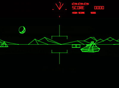
This looks a LOT like 1980’s laser projection graphics (or even 2020 laser projection graphics for that matter) because it is essentially drawn the same way – like an Etch-a-Sketch. What you see is traced by a beam. Internally it is more of a ‘connect the dots’ system, with the beam jumping from point to point (look closely at the dark side of the moon in the image above and you can see the dots). If the beam is ‘blanked’, or off, we don’t see the jump from one point to the next. But if the beam is on, we see a visible line.
Now for the video side. Most modern video cameras use a ‘raster’ system. An image is made from horizontal lines, each containing a fixed number of dots, or pixels. When you see a rating for, say, “8 megapixels” on a camera, that just means that when you multiply the pixels per line by the number of lines, you get eight million(ish). Video and TV’s tend to be specified differently, but it is the same basic thing. Instead of the total number of pixels, they tend to refer to just one dimension. A 1080p setting on your TV is 1920 x 1080 pixels. A 4K image is 4096 x 2160 for production equipment.
Making things more complicated, the entire raster image is not captured at exactly the same time. Generally one line is recorded at time, sort of like the way a scanner or photocopier captures a document, just faster. This is often called a “rolling shutter”. A decent video of how this works can be found here:
In general, a rolling shutter combined with a fast oscillation, like our laser projector, is a problem. It causes projected images to flicker, have dark gaps, distort, etc. in the recorded video. But a rolling shutter can also make for some great effects. Like the iphone inside a guitar video that went viral back in 2011:
We want to do something similar. We want to make artifacts of a rolling shutter combined with projected laser graphics controlled and reproducible. But before we do that, we’ll need to flesh out some technology pieces.
Next up: We’ll meet a modern laser projector