In the last post we met an ILDA laser projector and got a glimpse of the rolling shutter/scanning image problem we are looking to address. Now we need to put together a controller to drive the projector.
When I last worked on laser control 35 years ago the system used a Zilog Z80 CPU running at 4 MHz. The scan rate was about 14 kHz (70 uS per XY coordinate). If you check the processor manual from Zilog you will see that an instruction fetch took 4 clock cycles, so there were only 70 instruction fetches per coordinate pair available.
With only 70 instruction fetches available a big chunk of available CPU time was spent just getting each new XY coordinate pair from EPROM memory (memory chips with little windows we would erase with UV light) and out to DACs (Digital to Analog Converters). When you consider that the Z80 had no hardware multiplication built in (multiplication was done by repeatedly adding), and the obvious question is, how did the system rotate images around the X, Y, and Z axes in real time?
The secret ingredient was a card with 16 “multiplying DACs”. In a sense, all DACs are multiplying. They have a reference voltage and you input a digital value that causes some fraction of that reference voltage to be output. Essentially, you can think of the DAC as multiplying the reference voltage by a value from 0 to 1.0.
But Multiplying DACs are constructed so that their voltage references can be adjusted over a wide range, including 0V. So the output of one DAC can be fed to the reference of another. Let’s see how this might work for something simple like controlling image size.
First, we’ll start with a connect-the-dots fox:
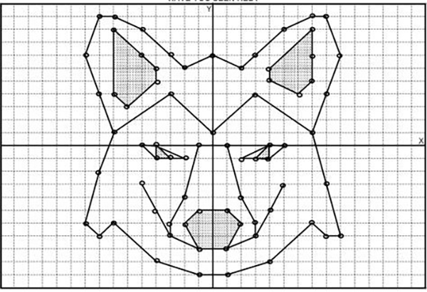
To make him bigger or smaller, we need to adjust all the dots by some scale. If we make the center of the graph 0, 0, the tip of his ear on the right is at 8x, 10y (8 ticks right from center on the X axis, 10 ticks up from center on the Y axis) and the bottom left of his face is -9x, -6y (9 ticks left of center on the X axis, 6 ticks down from center on the Y axis).
Scaling these coordinate is simple. We just multiply. For a scale of 1.0, we get the original coordinates.
[8, 10] x 1 = [8, 10]
[-9, -6] x 1 = [-9, -6]
To scale down to half size, we can multiply by 0.5.
[8, 10] x 0.5 = [4, 5]
[-9, -6] x 0.5 = [-4.5, -3]
To scale up to double size, we could multiply by 2.0. To invert the image on both axes we could multiply by -1.0. As I said, simple but, again, CPU power used to be very limited. So let’s see how we might solve scaling with 3 multiplying DACs:
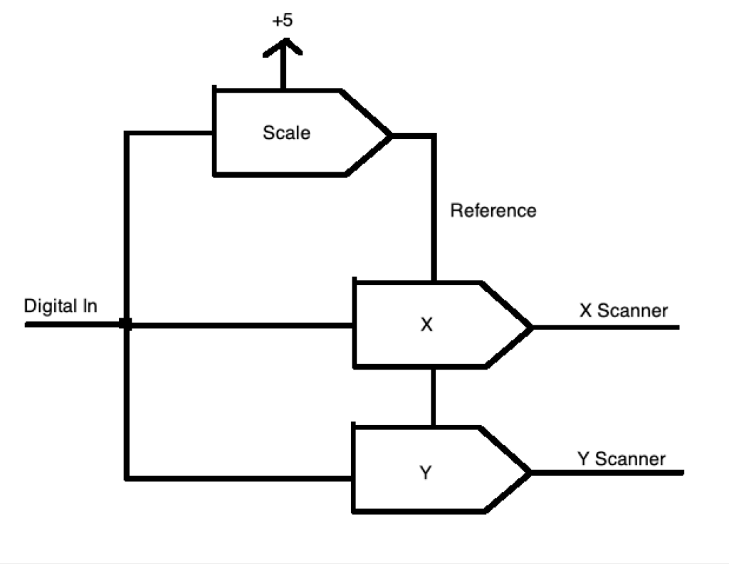
In this case we write our desired size to the scale multiplying DAC once. Then write unaltered X and Y values to their respective DAC channels. The scale channel will alter the reference for the two other DACs from 0 to 5V. Our X and Y values then become a percentage, or scale, of that reference.
This same concept can be extended to a Rotation Matrix, which uses multiplication and addition to move points in Euclidean space, but we’ll cover those in detail in a later post .
For now, let’s just be thankful that CPU power has become a lot more plentiful! We are looking to do something pretty generic and reusable, so I am going to start with an ARM core processor. ARM cores are exceedingly popular and offered by many different MCU manufacturers, so we’ll have lots of choices moving forward. Because of ARM’s popularity, the free tools are also pretty well developed.
There are lots of good choices, but I’m going with an offering from ST. I’ve used a number of different ARM families from different companies, and almost any of them would work fine, but I like some of the MCU peripherals, particularly timers, in the STM32Fxxx family parts quite a bit and, again, ST is pretty well supported by the free tools.
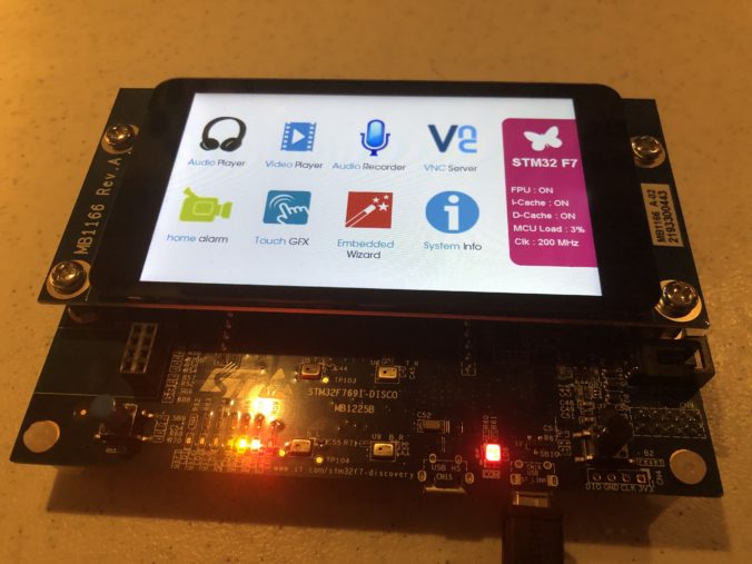
Instead of building a board from scratch, let’s just go with a development board. I’ve selected this one, which is also pictured at the top of this post. It’s got pretty much all the basic IO we might want, like Ethernet, a USB connection, a micro-SD card slot, and a spiffy little color display with a touch screen on it – all for $89. You can also buy the same card without the display for $49.
The MCU runs at 200 MHz, which probably sounds slow by today’s standards, but it is actually more than 50x faster than our Z80 above. The MCU has a faster instruction pipeline, so even if we scan at 60 kHz, we have about 3,300 cycles available to process each point. Further, the part contains both a hardware double precision FPU (floating point unit) and supports something called the “ARM DSP Instructions“, basically 16 an 32 bit integer multiplies and adds in a single cycle.
Some other nice feature are that it has ARDUINO compatible expansion connectors on the back for us to add our ILDA interface support:
And it has a built in programmer/debugger, called ST-Link, so we don’t have to buy an additional JTAG interface to do development (well, yes, I already have a SEEGER J-Link for work, but you might not, and they are a few hundred bucks).
Speaking of development, most the sample code from ST comes setup for the Keil and IAR ARM compiler environments. As it happens, I have access to both of these, but since this is all open source, we’ll stick with the free GNU GCC ARM compiler.
Debugging from a terminal window is doable, but a massive pain, so let’s cobble together an IDE environment for the GCC toolchain using Eclipse. It’s not a great IDE, but its free. In addition to the toolchain above and our IDE, we’ll need a way to connect the GCC debugger to our ST-Link debugging probe built in to the eval board. For that we can use OpenOCD.
It is certainly possible to pull all these pieces together and make them work via primal screams and trial and error, but a somewhat integrated set of instructions can be found here:
https://gnu-mcu-eclipse.github.io/
This project contains some additional CDT plug-in’s for Eclipse that I’ve never really used, but also some project templates for STM32Fxxx based processors and boards that are very handy, not just for getting a base project setup, but also for linking in some of the ST peripheral support library code.
I just setup everyone on OS X, because I like working in it better, but there is no reason you couldn’t setup to build under Windows.
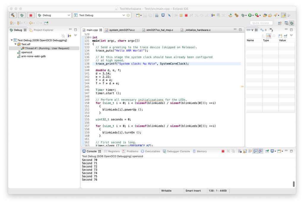
Above I took the basic ‘blinky’ skeleton, modified it so it was on the right IO pin for an LED on the eval board, and turned on and tested the FPU. If you would like to play with the board and MCU yourself, two critical documents are the MCU datasheet and the reference manual. Both of which can be found here.
ST Micro also has a pretty extensive collection of sample code and applications for the processor family and this specific eval board on GitHub.
[Edit] Don’t bother with the GitHub versions. For various licensing reasons parts are excluded and some of the main samples won’t build. You have to fill out a registration and agree to a different license agreement, but get the code directly from st.com.
Next up, we’ll need to start adding some IO!
Leave a Reply